10©2018 Integrated Device Technology, Inc. May 30, 2018
9FGV1005 Datasheet
1
Single CMOS driver active for each output pair.
2
See Test Loads for details.
3
I
DDCORE
= I
DDA
+ I
DDD.
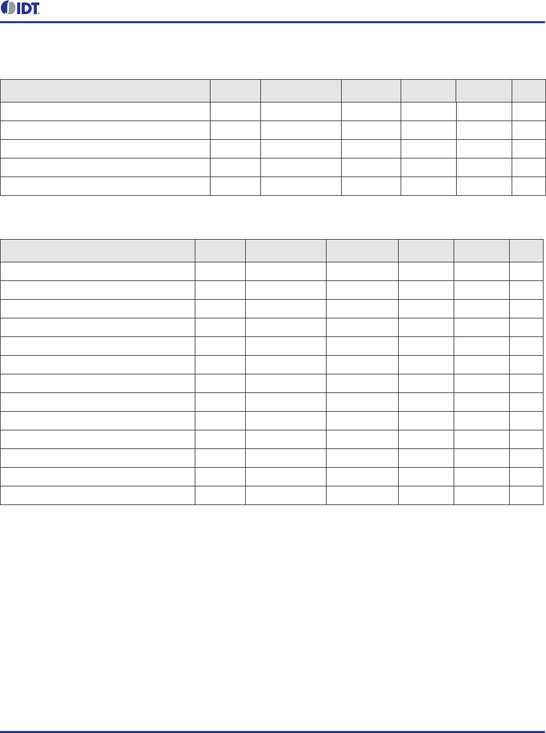
Table 12. Current Consumption
V
DDO
= 3.3V ±5%, 2.5V ±5%, 1.8V ±5%, T
A
= -40°C to +85°C unless stated otherwise.
Parameter Symbol Conditions Minimum Typical Maximum Units Notes
V
DDREF
Supply Current
I
DDREF
50MHz REFCLK. 5 8 mA
Core Supply Current I
DDCORE
2500MHz VCO, 50MHz REFCLK. 24 31 mA 3
Output Buffer Supply
Current (V
DDO1
)
I
DDO
x
LVDS, 325MHz. 22 28 mA 2
LP-HCSL, 100MHz. 17 24 mA 2
LVCMOS, 50MHz. 15 20 mA 1,2
LVCMOS, 200MHz. 25 40 mA 1,2
Output Buffer Supply
Current (V
DDO0)
LVDS, 325MHz. 8 12 mA 2
LP-HCSL. 6 10 mA 2
LVCMOS, 50MHz. 4 7 mA 1,2
LVCMOS, 200MHz. 13 26 mA 1,2
Total Power Down Current I
DDPD
Programmable outputs in HCSL
mode, B37[6,0] = 0.
710mA2
Programmable outputs in LVDS
mode, B37[6,0] = 0.
16 21 mA 2
Programmable outputs in
LVCMOS1 mode, B37[6,0] = 0.
57mA2
11©2018 Integrated Device Technology, Inc. May 30, 2018
9FGV1005 Datasheet
I
2
C Bus Characteristics
Note: A device must internally provide a hold time of at least 300ns for the SDA signal (referred to the V
IH(MIN)
of the SCL signal) to bridge the
undefined region of the falling edge of SCL.
Table 13. I
2
C Bus DC Characteristics
Parameter Symbol Conditions Minimum Typical Maximum Units
Input High Level V
IH
0.7 x V
DDD
V
Input Low Level V
IL
0.3 x V
DDD
V
Hysteresis of Inputs V
HYS
—0.05 x V
DDD
V
Input Leakage Current I
IN
—-1 30μA
Output Low Voltage V
OL
I
OL
= 3mA. 0.4 V
Table 14. I
2
C Bus AC Characteristics
Parameter Symbol Conditions Minimum Typical Maximum Units
Serial Clock Frequency (SCL) F
SCLK
10 400 kHz
Bus free time between STOP and START t
BUF
—1.3 μs
Setup Time, START t
SU:START
—0.6 μs
Hold Time, START t
HD:START
—0.6 μs
Setup Time, Data Input (SDA) t
SU:DATA
—0.1 μs
Hold Time, Data Input (SDA) 1 t
HD:DATA
—0 μs
Output Data Valid from Clock t
OVD
—0.9μs
Capacitive Load for Each Bus Line C
B
400 pF
Rise Time, Data and Clock (SDA, SCL) t
R
20 + 0.1 x C
B
300 ns
Fall Time, Data and Clock (SDA, SCL) t
F
20 + 0.1 x C
B
300 ns
High Time, Clock (SCL) t
HIGH
—0.6 μs
Low Time, Clock (SCL) t
LOW
—1.3 μs
Setup Time, STOP t
SU:STOP
—0.6 μs
12©2018 Integrated Device Technology, Inc. May 30, 2018
9FGV1005 Datasheet
Crystal Characteristics
Package Outline Drawings
The package outline drawings are appended at the end of this document and are also accessible from the link below. The package
information is the most current data available and is subject to change without notice or revision of this document.
www.idt.com/document/psc/16-lga-package-outline-drawing-30-x-30-x-110-mm-body-05mm-pitch-ltg16p1
Marking Diagrams
Table 15. Recommended Crystal Characteristics
Parameter Value Units
Frequency
8–50 MHz
Resonance Mode
Fundamental -
Frequency Tolerance at 25°C
±20 ppm maximum
Frequency Stability, REF at 25°C Over Operating Temperature Range
±20 ppm maximum
Temperature Range (commercial)
0–70 °C
Temperature Range (industrial)
-40–85 °C
Equivalent Series Resistance (ESR)
50 maximum
Shunt Capacitance (C
O
)
7 pF maximum
Load Capacitance (C
L
)
8 pF maximum
Drive Level
0.1 mW maximum
Aging per year
±5 ppm maximum
1. Line 1: truncated part number
2. “YWW” denotes the last digits of the year and week the part was assembled.
3. “$” denotes mark code.
4. “XXX” denotes lot number.
5000I
YWW$
XXX
5500I
YWW$
XXX

9FGV1005Q507LTGI

Mfr. #:
Manufacturer:
IDT
Description:
Clock Generators & Support Products 9FGV1005 W/INT 50MHZ XTAL
Lifecycle:
New from this manufacturer.
Delivery:
DHL FedEx Ups TNT EMS
Payment:
T/T Paypal Visa MoneyGram Western Union