4©2018 Integrated Device Technology, Inc. May 30, 2018
9FGV1005 Datasheet
Absolute Maximum Ratings
The absolute maximum ratings are stress ratings only. Stresses greater than those listed below can cause permanent damage to the
device. Functional operation of the 9FGV1005 at absolute maximum ratings is not implied. Exposure to absolute maximum rating
conditions may affect device reliability.
Thermal Characteristics
1
EPAD soldered to board.
Table 2. Absolute Maximum Ratings
Parameter Rating
Supply Voltage, V
DDA
, V
DDD
, V
DDO
3.465V
Storage Temperature, T
STG
-65°C to 150°C
ESD Human Body Model 2000V
Junction Temperature 125°C
Inputs
XIN/CLKIN 0V to 1.2V voltage swing
Other Inputs -0.5V to V
DDD
Outputs
Outputs, V
DDO
(LVCMOS) -0.5V to V
DDO
+ 0.5V
Outputs, IO (SDA) 10mA
Table 3. Thermal Characteristics
1
Parameter Symbol Conditions Package Typical Values Units Notes
Thermal Resistance
(devices with external crystal)
θ
JC
Junction to case.
LTG16
66 °C/W 1
θ
Jb
Junction to base. 5.1 °C/W 1
θ
JA0
Junction to air, still air. 63 °C/W 1
θ
JA1
Junction to air, 1 m/s air flow. 56 °C/W 1
θ
JA3
Junction to air, 3 m/s air flow. 51 °C/W 1
θ
JA5
Junction to air, 5 m/s air flow. 49 °C/W 1
Thermal Resistance
Q-series (devices with internal
crystal)
θ
JC
Junction to case.
LTG16
82.1 °C/W 1
θ
Jb
Junction to base. 42.3 °C/W 1
θ
JA0
Junction to air, still air. 93.6 °C/W 1
θ
JA1
Junction to air, 1 m/s air flow. 87.1 °C/W 1
θ
JA3
Junction to air, 3 m/s air flow. 83.3 °C/W 1
5©2018 Integrated Device Technology, Inc. May 30, 2018
9FGV1005 Datasheet
Recommended Operating Conditions
Electrical Characteristics
V
DDx
= 3.3V ±5%, 2.5V ±5%, 1.8V ±5%, T
A
= -40°C to +85°C unless stated otherwise.
Table 4. Recommended Operating Conditions
Symbol Parameter Minimum Typical Maximum Units
V
DDOx
Power supply voltage for supporting 1.8V outputs. 1.71 1.8 1.89 V
Power supply voltage for supporting 2.5V outputs. 2.375 2.5 2.625 V
Power supply voltage for supporting 3.3V outputs. 3.135 3.3 3.465 V
V
DDD
Power supply voltage for core logic functions. 1.71 3.465 V
V
DDA
Analog power supply voltage. Use filtered analog power supply if
available.
1.71 3.465 V
T
A
Operating temperature, ambient. -40 85 °C
C
L
Maximum load capacitance (3.3V LVCMOS only). 15 pF
t
PU
Power-up time for all V
DD
s to reach minimum specified voltage (power
ramps must be monotonic).
0.05 5 ms
Table 5. Common Electrical Characteristics
Parameter Symbol Conditions Minimum Typical Maximum Units Notes
Input Frequency f
IN
Crystal input frequency. 8 50 MHz 1
CLKIN input frequency. 1 240 MHz 5
Output Frequency f
OUT
Differential clock output. 10 325 MHz
Single-ended clock output. 10 200 MHz
VCO Frequency f
VCO
VCO operating frequency range. 2400 2500 2600 MHz
Loop Bandwidth f
BW
Input frequency = 25MHz. 0.06 0.9 MHz
Input High Voltage V
IH
SEL[1:0]. 0.7 x V
DDD
V
DDD
+ 0.3 V
Input Low Voltage V
IL
SEL[1:0]. GND - 0.3 0.8 V
Input High Voltage V
IH
REF/SEL_I2C#. 0.65 x V
DDREF
V
DDREF
+ 0.3 V
Input Low Voltage V
IL
REF/SEL_I2C#. -0.3 0.4 V
Input High Voltage V
IH
XIN/CLKIN. 0.8 1.2 V
Input Low Voltage V
IL
XIN/CLKIN. -0.3 0.4 V
Input Rise/Fall Time T
R
/T
F
SEL1/SDA, SEL0/SCL. 300 ns
Input Capacitance C
IN
SEL[1:0]. 3 7 pF
Internal Pull-up
Resistor
R
UP
SEL[1:0] at 25°C. 200 237 300 k
Internal Pull-down
Resistor
R
DOWN
REF/SEL_I2C#. 200 237 300 k
6©2018 Integrated Device Technology, Inc. May 30, 2018
9FGV1005 Datasheet
1
Practical lower frequency is determined by loop filter settings.
2
Includes loading the configuration bits from OTP to registers.
3
Actual PLL lock time depends on the loop configuration.
4
Actual jitter is configuration dependent. These values are representative of what the device can achieve.
5
Input doubler off. Maximum input frequency with input doubler on is 160MHz.
1
This configuration used for 12kHz–20MHz phase jitter measurement.
2
This configuration used for PCIe filtered phase jitter measurements.
3
Outputs configured as LP-HCSL or LVDS with REF output off, unless noted.
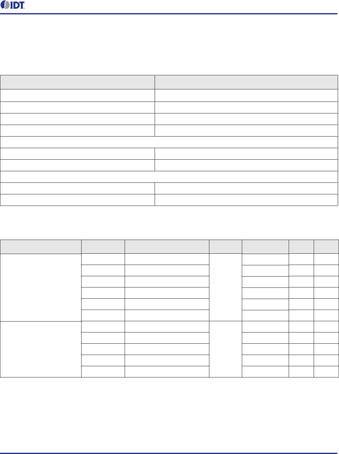
Programmable
Capacitance at XIN and
XO (XIN in parallel with
XO)
C
L
XIN/CLKIN, XO. 0 8 pF
Input Duty Cycle t2 CLKIN, measured at V
DDREF
/2. 40 50 60 %
Output Duty Cycle t3
LVCMOS, f
OUT
> 156.25MHz. 40 50 60 %
LVCMOS, f
OUT
156.25MHz. 45 50 55 %
LVDS, LP-HCSL outputs. 45 50.2 55 %
Clock Jitter t6
Cycle-to-cycle jitter (peak-to-peak),
See “Test Frequencies for Jitter
Measurements in Common Electrical
Characteristics” for configurations.
30 50 ps 4
Reference clock RMS phase jitter
(12kHz to 5MHz integration range).
See “Test Frequencies for Jitter
Measurements in Common Electrical
Characteristics” for configurations.
284
fs
rms
4
OUTx RMS phase jitter(12kHz to
20MHz integration range) differential
output. See “Test Frequencies for
Jitter Measurements in Common
Electrical Characteristics” for
configurations.
259
fs
rms
4
Output Skew t7
Skew between the same frequencies,
with outputs using the same driver
format.
37 50 ps
Lock Time t8 PLL lock time from power-up. 5 10 ms 2,3
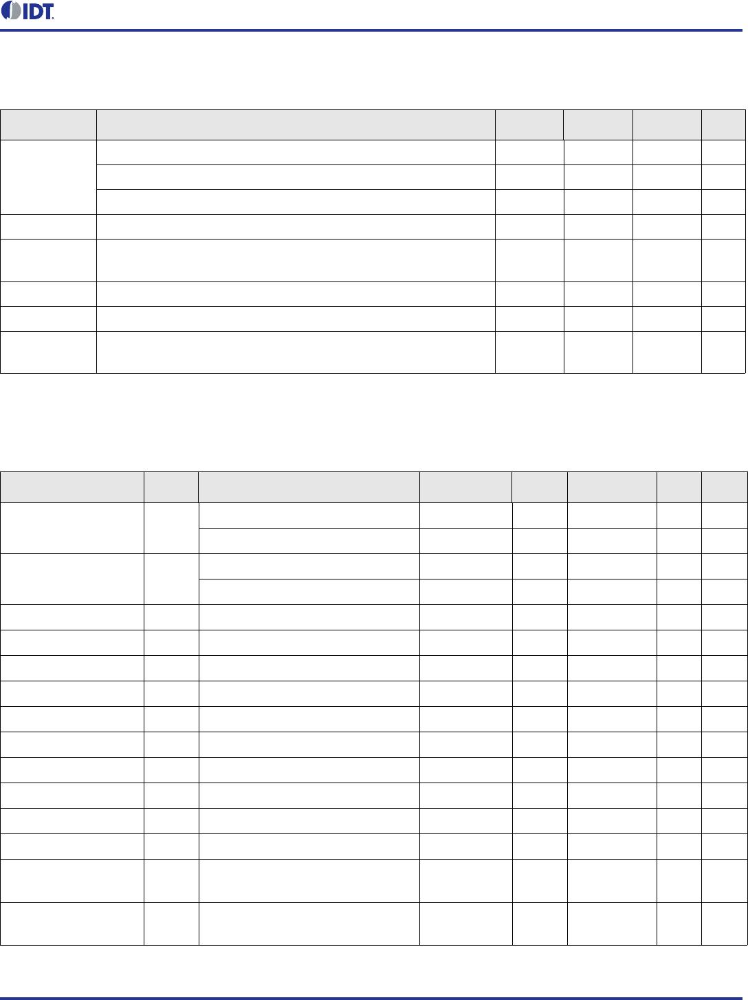
Table 6. Test Frequencies for Jitter Measurements in Common Electrical Characteristics Table
V
DDx
= 3.3V ±5%, 2.5V ±5%, 1.8V ±5%, T
A
= -40°C to +85°C unless stated otherwise.
Device XIN/CLKIN OUT0 OUT1 Unit Notes
9FGV1005 50 156.25 MHz 1,3
9FGV1005Q5 50 100 MHz 2,3
Table 5. Common Electrical Characteristics (Cont.)
Parameter Symbol Conditions Minimum Typical Maximum Units Notes

9FGV1005Q507LTGI

Mfr. #:
Manufacturer:
IDT
Description:
Clock Generators & Support Products 9FGV1005 W/INT 50MHZ XTAL
Lifecycle:
New from this manufacturer.
Delivery:
DHL FedEx Ups TNT EMS
Payment:
T/T Paypal Visa MoneyGram Western Union