Precision Thermocouple Amplifiers
with Cold Junction Compensation
AD8494/AD8495/AD8496/AD8497
Rev. C
Information furnished by Analog Devices is believed to be accurate and reliable. However, no
responsibility is assumed by Analog Devices for its use, nor for any infringements of patents or other
rights of third parties that may result from its use. Specifications subject to change without notice. No
license is granted by implication or otherwise under any patent or patent rights of Analog Devices.
Trademarks and registered trademarks are the property of their respective owners.
One Technology Way, P.O. Box 9106, Norwood, MA 02062-9106, U.S.A.
Tel: 781.329.4700 www.analog.com
Fax: 781.461.3113 ©2010–2011 Analog Devices, Inc. All rights reserved.
FEATURES
Low cost and easy to use
Pretrimmed for J or K type thermocouples
Internal cold junction compensation
High impedance differential input
Standalone 5 mV/°C thermometer
Reference pin allows offset adjustment
Thermocouple break detection
Laser wafer trimmed to 1°C initial accuracy and
0.025°C/°C ambient temperature rejection
Low power: <1 mW at V
S
= 5 V
Wide power supply range
Single supply: 2.7 V to 36 V
Dual supply: ±2.7 V to ±18 V
Small, 8-lead MSOP
APPLICATIONS
J or K type thermocouple temperature measurement
Setpoint controller
Celsius thermometer
Universal cold junction compensator
White goods (oven, stove top) temperature measurements
Exhaust gas temperature sensing
Catalytic converter temperature sensing
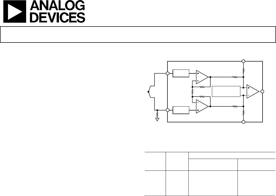
FUNCTIONAL BLOCK DIAGRAM
–IN
+IN
OUT
REF
08529-001
A1
A2
AD8494/AD8495/
AD8496/AD8497
A3
SENSE
ESD AND
OVP
ESD AND
OVP
COLD JUNCTION
COMPENSATION
1M
THERMO-
COUPLE
Figure 1.
Table 1. Device Temperature Ranges
Optimized Temperature Range
Part No.
Thermo-
Couple
Type
Ambient Temperature
(Reference Junction)
Measurement
Junction
AD8494 J 0°C to 50°C Full J type range
AD8495 K 0°C to 50°C Full K type range
AD8496 J 25°C to 100°C Full J type range
AD8497 K 25°C to 100°C Full K type range
GENERAL DESCRIPTION
The AD8494/AD8495/AD8496/AD8497 are precision
instrumentation amplifiers with thermocouple cold junction
compensators on an integrated circuit. They produce a high
level (5 mV/°C) output directly from a thermocouple signal by
combining an ice point reference with a precalibrated amplifier.
They can be used as standalone thermometers or as switched
output setpoint controllers using either a fixed or remote
setpoint control.
The AD8494/AD8495/AD8496/AD8497 can be powered from a
single-ended supply (less than 3 V) and can measure temperatures
below 0°C by offsetting the reference input. To minimize self-
heating, an unloaded AD849x typically operates with a total
supply current of 180 µA, but it is also capable of delivering in
excess of ±5 mA to a load.
The AD8494 and AD8496 are precalibrated by laser wafer
trimming to match the characteristics of J type (iron-constantan)
thermocouples; the AD8495 and AD8497 are laser trimmed to
match the characteristics of K type (chromel-alumel) thermo-
couples. See Table 1 for the optimized ambient temperature
range of each part.
The AD8494/AD8495/AD8496/AD8497 allow a wide variety of
supply voltages. With a 5 V single supply, the 5 mV/°C output
allows the devices to cover nearly 1000 degrees of a thermo-
couples temperature range.
The AD8494/AD8495/AD8496/AD8497 work with 3 V supplies,
allowing them to interface directly to lower supply ADCs. They
can also work with supplies as large as 36 V in industrial systems
that require a wide common-mode input range.
PRODUCT HIGHLIGHTS
1. Complete, precision laser wafer trimmed thermocouple
signal conditioning system in a single IC package.
2. Flexible pinout provides for operation as a setpoint
controller or as a standalone Celsius thermometer.
3. Rugged inputs withstand 4 kV ESD and provide over-
voltage protection (OVP) up to V
S
± 25 V.
4. Differential inputs reject common-mode noise on the
thermocouple leads.
5. Reference pin voltage can be offset to measure 0°C on
single supplies.
6. Available in a small, 8-lead MSOP that is fully RoHS compliant.
AD8494/AD8495/AD8496/AD8497
Rev. C | Page 2 of 16
TABLE OF CONTENTS
Features .............................................................................................. 1
Applications....................................................................................... 1
Functional Block Diagram .............................................................. 1
General Description......................................................................... 1
Product Highlights ........................................................................... 1
Revision History ............................................................................... 2
Specifications..................................................................................... 3
Absolute Maximum Ratings............................................................ 5
Thermal Resistance ...................................................................... 5
ESD Caution.................................................................................. 5
Pin Configuration and Function Descriptions............................. 6
Typical Performance Characteristics ............................................. 7
Theory of Operation ...................................................................... 11
Thermocouples........................................................................... 11
Thermocouple Signal Conditioner.......................................... 11
AD8494/AD8495/AD8496/AD8497 Architecture .................. 11
Maximum Error Calculation.................................................... 12
Recommendations for Best Circuit Performance.................. 13
Applications Information.............................................................. 14
Basic Connection ....................................................................... 14
Ambient Temperature Sensor................................................... 14
Setpoint Controller .................................................................... 15
Measuring Negative Temperatures .......................................... 15
Reference Pin Allows Offset Adjustment................................ 15
Outline Dimensions ....................................................................... 16
Ordering Guide .......................................................................... 16
REVISION HISTORY
6/11—Rev. B to Rev. C
Changes to Figure 35 and Figure 36............................................. 15
4/11—Rev. A to Rev. B
Changes to Figure 1.......................................................................... 1
Changes to Figure 33 and Figure 34............................................. 14
Changes to Figure 35 and Figure 36............................................. 15
Changes to Ordering Guide .......................................................... 16
10/10—Rev. 0 to Rev. A
Changes to Linearity Error of the Thermocouple Section........ 12
Changes to Ambient Temperature Sensor Section .................... 14
Changes to Ordering Guide .......................................................... 16
7/10—Revision 0: Initial Version
AD8494/AD8495/AD8496/AD8497
Rev. C | Page 3 of 16
SPECIFICATIONS
+V
S
= 5 V, −V
S
= 0 V, V
+IN
= V
−IN
= 0 V, V
REF
= 0 V, T
A
= T
RJ
= 25°C, R
L
= 100 k, unless otherwise noted. Specifications do not include
gain and offset errors of the thermocouple itself. T
A
is the ambient temperature at the AD849x; T
RJ
is the thermocouple reference junction
temperature; T
MJ
is the thermocouple measurement junction temperature.
Table 2.
A Grade C Grade
Parameter Test Conditions/Comments Min Typ Max Min Typ Max Unit
TEMPERATURE ACCURACY
Initial Accuracy
AD8494/AD8495 T
A
= T
RJ
= T
MJ
= 25°C 3 1 °C
AD8496/AD8497 T
A
= T
RJ
= 60°C, T
MJ
= 175°C 3 1.5 °C
Ambient Temperature
Rejection
1
AD8494/AD8495 T
A
= T
RJ
= 0°C to 50°C 0.05 0.025 °C/°C
AD8496/AD8497 T
A
= T
RJ
= 25°C to 100°C 0.05 0.025 °C/°C
Gain Error
2,
3
V
OUT
= 0.125 V to 4.125 V
AD8494/AD8495 0.3 0.1 %
AD8496/AD8497 0.3 0.1 %
Transfer Function 5 5 mV/°C
INPUTS
Input Voltage Range −V
S
– 0.2 +V
S
– 1.6 −V
S
– 0.2 +V
S
– 1.6 V
Overvoltage Range +V
S
– 25 −V
S
+ 25 +V
S
– 25 −V
S
+ 25 V
Input Bias Current
4
25 50 25 50 nA
Input Offset Current 1.5 0.5 nA
Common-Mode Rejection V
CM
= 0 V to 3 V 1 0.3 °C/V
Power Supply Rejection +V
S
= 2.7 V to 5 V 0.5 0.5 °C/V
NOISE
Voltage Noise f = 0.1 Hz to 10 Hz, T
A
= 25°C 0.8 0.8 μV p-p
Voltage Noise Density f = 1 kHz, T
A
= 25°C 32 32 nV/√Hz
Current Noise Density f = 1 kHz, T
A
= 25°C 100 100 fA/√Hz
REFERENCE INPUT
Input Resistance 60 60
Input Current 25 25 μA
Voltage Range −V
S
+V
S
−V
S
+V
S
V
Gain to Output 1 1 V/V
OUTPUT
Output Voltage Range −V
S
+ 0.025 +V
S
– 0.1 −V
S
+ 0.025 +V
S
– 0.1 V
Short-Circuit Current
5
7 7 mA
DYNAMIC RESPONSE
−3 dB Bandwidth
AD8494 30 30 kHz
AD8495/AD8497 25 25 kHz
AD8496 31 31 kHz
Settling Time to 0.1% 4 V output step
AD8494 36 36 μs
AD8495/AD8497 40 40 μs
AD8496 32 32 μs
POWER SUPPLY
Operating Voltage Range
6
Single Supply 2.7 36 2.7 36 V
Dual Supply ±2.7 ±18 ±2.7 ±18 V
Quiescent Current 180 250 180 250 μA

AD8495CRMZ

Mfr. #:
Manufacturer:
Analog Devices Inc.
Description:
Board Mount Temperature Sensors Thermocouple Amp w/Cold Jct Compensat
Lifecycle:
New from this manufacturer.
Delivery:
DHL FedEx Ups TNT EMS
Payment:
T/T Paypal Visa MoneyGram Western Union