DS28CM00: I²C/SMBus Silicon Serial Number
3 of 9
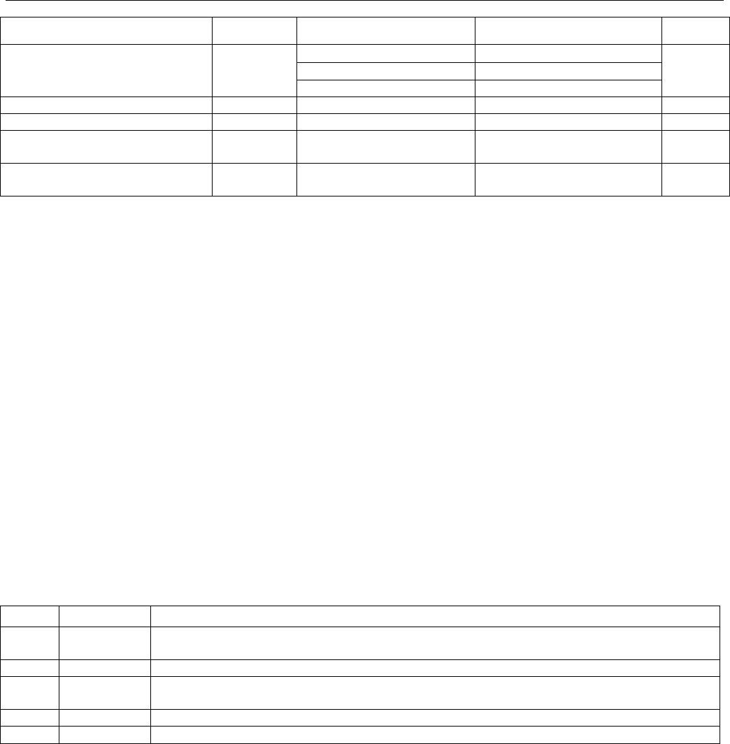
PARAMETER SYMBOL CONDITIONS MIN TYP MAX UNITS
V
CC
≥ 2.7V
0.3 0.9
V
CC
≥ 2.0V
0.3 1.1
Data Hold Time (Notes 9, 10) t
HD:DAT
V
CC
< 2.0V 0.3 1.7
µs
Data Setup Time t
SU:DAT
(Notes 8, 11) 100 ns
Setup Time for STOP Condition t
SU:STO
(Note 8) 0.6 µs
Bus Free Time Between a
STOP and START Condition
t
BUF
(Note 8) 1.3 µs
Capacitive Load for Each Bus
Line
C
b
(Notes 4, 8) 400 pF
Note 1:
Specifications at -40°C are guaranteed by design and characterization only and not production tested.
Note 2:
All values are referred to V
IHmin
and V
ILmax
levels.
Note 3:
The maximum specification value is guaranteed by design, not production tested.
Note 4:
Not production tested. Guaranteed by design or characterization.
Note 5:
C
B
= total capacitance of one bus line in pF. If mixed with HS-mode devices, faster fall-times according
to I
2
C-Bus Specification v2.1 are allowed.
Note 6:
The DS28CM00 does not obstruct the SDA and SCL lines if V
CC
is switched off.
Note 7:
The minimum SCL clock frequency is limited by the bus timeout feature. If the CM bit is 1 AND SCL
stays at the same logic level or SDA stays low for this interval, the DS28CM00 behaves as though it
has sensed a STOP condition.
Note 8:
System Requirement
Note 9:
The DS28CM00 provides a hold time of at least 300ns for the SDA signal (referred to the V
IHmin
of the
SCL signal) to bridge the undefined region of the falling edge of SCL.
Note 10:
The maximum t
HD:DAT
has only to be met if the device does not stretch the low period (t
LOW
) of the SCL
signal.
Note 11:
A Fast-mode I²C-bus device can be used in a standard-mode I²C-bus system, but the requirement
t
SU:DAT
≥ 250ns must then be met. This is automatically the case if the device does not stretch the LOW
period of the SCL signal. If such a device does stretch the LOW period of the SCL signal, it must
output the next data bit to the SDA line tr max + t
SU:DAT
= 1000 + 250 = 1250ns (according to the
standard-mode I²C-bus specification) before the SCL line is released.
PIN DESCRIPTION
PIN NAME FUNCTION
1 SCL
Serial interface clock input; must be tied to V
CC
through a pullup resistor. 5V tolerant input
over 1.62V to 5.25V V
CC
range.
2 GND Ground supply for the device.
3 SDA
Serial interface bi-directional data line; must be tied to V
CC
through a pullup resistor. 5V
tolerant input/output over 1.62V to 5.25V V
CC
range.
4 N.C. Not Connected
5 V
CC
Power Supply Input
OVERVIEW
The DS28CM00 consists of a serial interface which provides access to a unique 64-bit Registration number and a
Control Register, as shown in the block diagram in Figure 1. The device communicates with a host processor
through its SMBus compatible I²C bus interface in standard-mode or in fast-mode. Since the network address of
the DS28CM00 is fixed, exactly one device can reside on a bus segment. The Registration Number and Control
Register are located in a linear 9-byte address space (Figure 2).

