DS28CM00R-A00+T

DS28CM00: I²C/SMBus Silicon Serial Number
7 of 9
Not Acknowledged by Slave
A slave device may be unable to receive or transmit data, e.g., because it is busy. As a SMBus-compatible device,
the DS28CM00 will always acknowledge its slave address. However, some time later the slave may refuse to
accept data, e.g., because of an invalid memory address or access mode, e. g. attempting to write to a ROM byte.
In this case the slave device will not acknowledge any of the bytes that it refuses and will leave SDA HIGH. After a
slave has failed to acknowledge, the master should generate a repeated START condition or a STOP condition
followed by a START condition to begin a new data transfer.
Not Acknowledged by Master
At some time when receiving data, the master must signal an end of data to the slave device. To achieve this, the
master does not acknowledge the last byte that it has received from the slave. In response, the slave releases
SDA, allowing the master to generate the STOP condition.
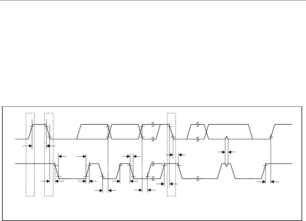
Figure 5. I²C/SMBus Timing Diagram
SCL
SDA
STOP START
t
BUF
t
HD:STA
t
LOW
t
R
t
HD:DAT
t
HIGH
t
SU:DAT
Repeated
START
t
SU:STA
t
F
t
HD:STA
t
SP
t
SU:STO
Spike
Suppression
NOTE: Timing is referenced to V
ILMAX
and V
IHMIN
.
Read and Write
The DS28CM00 behaves like an I²C memory device with an 9-byte memory map (Figure 2). The memory consists
of 8 bytes ROM and one byte SRAM, i. e., the Control Register. The ROM data cannot be changed.
To write to the DS28CM00, the master must access the device in write access mode, i.e., the slave address must
be sent with the direction bit set to 0. The next byte to be sent in write access mode is an address byte to set the
address pointer to a specific location. The DS28CM00 acknowledges any address between 00h and 08h. Write
attempts to the ROM are ignored and data received for these addresses is not acknowledged. However, the
address pointer increments after every full data byte transmitted by the master and rolls over from 08h to 00h after
a full data byte is written to address 08h.
To read from the DS28CM00, the master must access the device in read access mode, i.e., the slave address
must be sent with the direction bit set to 1. The address pointer determines the location from which the master will
start reading. The pointer is set when the DS28CM00 is accessed in write access mode, as described above. The
power-on default of the pointer is 00h. When reading from the device, the address pointer increments with every
data byte read. When the end of the memory is reached (address 08h), the address pointer wraps around to 00h.
To read from an arbitrary address, the master must first access the DS28CM00 in write access mode and specify a
new memory address. The address pointer remains unchanged if the device resets its communication interface
due to a bus timeout in SMBus mode.
DS28CM00: I²C/SMBus Silicon Serial Number
8 of 9
I²C CommunicationLegend
SYMBOL DESCRIPTION SYMBOL DESCRIPTION
S START Condition A Acknowledged
AD,0 Select DS28CM00 for Write Access A\ Not Acknowledged
AD,1 Select DS28CM00 for Read Access <byte> Transfer of One Byte
Sr Repeated START Condition VMA Valid Memory Address (00h to 08h)
P STOP Condition IMA Invalid Memory Address
Command-Specific CommunicationColor-Codes
Master-to-Slave Slave-to-Master
Communication Examples
Write to Control Register (address 08)
S AD,0 A 08h A <byte> A P
Write to ROM Address (excludes address 08)
S AD,0 A VMA A <byte> A\ P
Write to invalid address (>08)
S AD,0 A IMA A\ P
Read
S AD,0 A VMA A Sr AD,1 A <byte> A <byte> A\ P
Application Information
SDA and SCL Pullup Resistors
SDA is an open-drain output on the DS28CM00 that requires a pullup resistor (Figure 6) to realize high logic levels.
Because the DS28CM00 uses SCL only as input (no clock stretching) the master can drive SCL either through an
open-drain/collector output with a pullup resistor or a push-pull output.
Pullup Resistor R
P
Sizing
According to the I²C specification, a slave device must be able to sink at least 3mA at a V
OL
of 0.4V. The SMBus
specification requires a current sink capability of 4mA at 0.4V. The DS28CM00 can sink at least 4mA at 0.4V V
OL
over its entire operating voltage range. This DC characteristic determines the minimum value of the pullup resistor:
Rpmin = (V
CC
- 0.4V)/4mA. With a maximum operating voltage of 5.25V, the minimum value for the pullup resistor
is 1.2kΩ. The "Minimum RP" line in Figure 7 shows how the minimum pullup resistor changes with the operating
(pullup) voltage.
last byte
one or
more bytes
data is not accepted
address is not accepted
Set address pointer
DS28CM00: I²C/SMBus Silicon Serial Number
9 of 9
Figure 6. Application Schematic
V
CC
SD
A
SCL
µC
GND
V
CC
SDA
SCL
DS28CM00
GND
R
P
R
P
V
CC
To additional
devices
For I²C systems, the rise time and fall time are measured from 30% to 70% of the pullup voltage. The maximum
bus capacitance C
B
is 400pF. The maximum rise time must not exceed 300ns. Assuming maximum rise time, the
maximum resistor value at any given capacitance C
B
is calculated as: R
PMAX
= 300ns/(C
B
*ln(7/3)). For a bus
capacitance of 400pF the maximum pullup resistor would be 885Ω.
Since a 885Ω pullup resistor, as would be required to meet the rise time specification and 400pF bus capacitance,
is lower than R
PMIN
at 5.25V, a different approach is necessary. The "Max. Load…" line in Figure 7 is generated by
first calculating the minimum pullup resistor at any given operating voltage ("Minimum R
P
" line) and then calculating
the respective bus capacitance that yields a rise time of 300ns.
Only for pullup voltages of 4V and lower can the maximum permissible bus capacitance of 400pF be maintained. A
reduced bus capacitance of 300pF is acceptable for the entire operating voltage range. The corresponding pullup
resistor value at the voltage is indicated by the "Minimum R
P
" line.
Figure 7. I²C Fast Speed Pullup Resistor Selection Chart
0
200
400
600
800
1000
1200
1.5 2 2.5 3 3.5 4 4.5 5
Pull-up Voltage
Minimum Rp (Ohms)
0
100
200
300
400
500
600
Load (pF)
"Minimum Rp" Max. Load at Min. Rp fast mode
PACKAGE INFORMATION
(The package drawing(s) in this data sheet may not reflect the most current specifications. For the latest package outline information, go to
www.maxim-ic.com/DallasPackInfo.)

DS28CM00R-A00+T

Mfr. #:
Manufacturer:
Maxim Integrated
Description:
Security ICs / Authentication ICs I2C/SMBus Silicon Serial Number
Lifecycle:
New from this manufacturer.
Delivery:
DHL FedEx Ups TNT EMS
Payment:
T/T Paypal Visa MoneyGram Western Union

Products related to this Datasheet