DS28CM00R-A00+T

DS28CM00: I²C/SMBus Silicon Serial Number
4 of 9
Figure 1. Block Diagram
SCL
SDA
ROM
Registration
Number
Control
Register
Serial
Interface
V
CC
GND
Figure 2. Memory Map
ADDRESS TYPE ACCESS DESCRIPTION
00h ROM Read Device Family Code (70h)
01h ROM Read Serial Number, bits 0 to 7
02h ROM Read Serial Number, bits 8 to 15
03h ROM Read Serial Number, bits 16 to 23
04h ROM Read Serial Number, bits 24 to 31
05h ROM Read Serial Number, bits 32 to 39
06h ROM Read Serial Number, bits 40 to 47
07h ROM Read CRC of Family Code and 48-bit Serial Number
08h SRAM R/W Control Register
Unique Registration Number
Each DS28CM00 has a unique Registration Number that is 64 bits long. The registration number begins with the
family code at address 00h followed by the 48-bit serial number (LS-byte at the lower address) and ends at
address 07h with the CRC (Cyclic Redundancy Check) of the first 56 bits. This CRC is generated using the
polynomial X
8
+ X
5
+ X
4
+ 1. Additional information about CRCs is available in Application Note 27. The ROM
Registration Number is not related to the I²C slave address of the device.
Control Register
The Control Register at address 08h allows switching between I²C mode and SMBus mode. Only the LS bit of this
register, referred to as the CM bit, has a function. The other 7 bits always read 0 and cannot be changed. When the
CM bit is set to 1 (power-on default), the device is in SMBus mode, which enables the bus timeout function. Setting
the CM bit to 0 puts the device in I²C mode, where the timeout function is disabled. In SMBus mode, the serial
interface times out and is internally reset if SCL is stuck (high or low) or if SDA is stuck low for the duration of
t
TIMEOUT
or longer. This reset turns the SDA line into an input, ensuring that the device is ready to recognize a
communication start condition.
ADDR b7 b6 b5 b4 b3 b2 b1 b0
08h
0 0 0 0 0 0 0 CM
DS28CM00: I²C/SMBus Silicon Serial Number
5 of 9
DEVICE OPERATION
Typically, the DS28CM00 is accessed after power-up to read the 64-bit Registration number, which may serve to
identify the object that the device is embedded in. Write access exists only to the Control Register. Read and write
access are controlled through the I²C/SMBus serial interface. See section Read and Write for details.
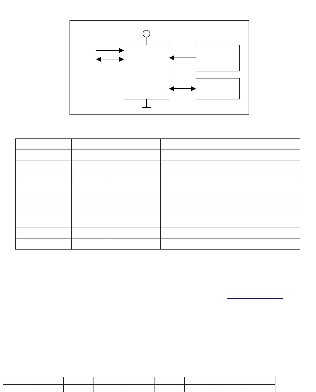
Serial Communication Interface
General Characteristics
The serial interface uses a data line (SDA) plus a clock signal (SCL) for communication. Both SDA and SCL are
bidirectional lines, connected to a positive supply voltage through a pullup resistor. When there is no
communication, both lines are HIGH. The output stages of devices connected to the bus must have an open-drain
or open-collector to perform the wired-AND function. Data can be transferred at rates of up to 100kbps in the
Standard-mode, up to 400kbps in the Fast-mode. The DS28CM00 works in both modes.
A device that sends data on the bus is defined as a transmitter, and a device receiving data as a receiver. The
device that controls the communication is called a “master.” The devices that are controlled by the master are
“slaves.” The DS28CM00 is a slave device.
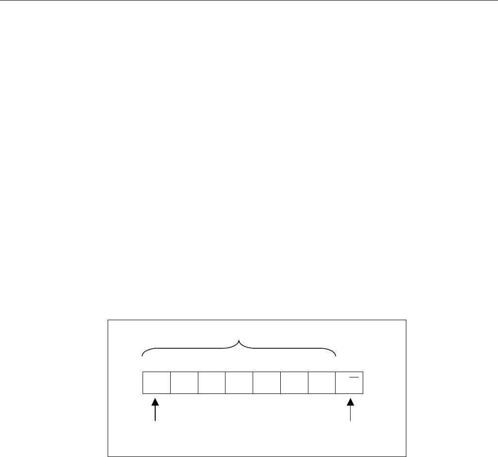
Slave Address/Direction Byte
To be individually accessed, each device must have a slave address that does not conflict with other devices on
the bus. The slave address to which the DS28CM00 responds is shown in Figure 3. The slave address is part of
the slave-address/direction byte. The last bit of the slave-address/direction byte (R/W) defines the data direction.
When set to a 0, subsequent data will flow from master to slave (write access mode); when set to a 1, data will flow
from slave to master (read access mode).
Figure 3. DS28CM00 Slave Address
A6 A5 A4 A3 A2 A1 A0
1 0 1 0 0 0 0 R/W
7-Bit Slave Address
Most Signi-
ficant Bit
Determines
Read or Write
I²C/SMBus Protocol
Data transfers may be initiated only when the bus is not busy. The master generates the serial clock (SCL),
controls the bus access, generates the START and STOP conditions, and determines the number of bytes
transferred between START and STOP (Figure 4). Data is transferred in bytes with the most significant bit being
transmitted first. After each byte follows an acknowledge bit to allow synchronization between master and slave.
During any data transfer, SDA must remain stable whenever the clock line is HIGH. Changes in SDA line while
SCL is high will be interpreted as a START or a STOP. The protocol is illustrated in Figure 4. For detailed timing
references see Figure 5.
DS28CM00: I²C/SMBus Silicon Serial Number
6 of 9
Figure 4. I²C/SMBus Protocol Overview
SCL
SDA
12 678
A
CK
9 912 8
MS-bit
R/
W
Slave Address
ACK
bit
Acknowledgment
from Receiver
ACK
bit
START
Condition
ACK
Repeated if more bytes
are transferred
STOP Condition
Repeated START
Condition
Idle
Bus Idle or Not Busy
Both, SDA and SCL, are inactive, i. e., in their logic HIGH states.
START Condition
To initiate communication with a slave, the master has to generate a START condition. A START condition is
defined as a change in state of SDA from HIGH to LOW while SCL remains HIGH.
STOP Condition
To end communication with a slave, the master has to generate a STOP condition. A STOP condition is defined as
a change in state of SDA from LOW to HIGH while SCL remains HIGH.
Repeated START Condition
Repeated starts are commonly used for read accesses to select a specific data source or address to read from.
The master can use a repeated START condition at the end of a data transfer to immediately initiate a new data
transfer following the current one. A repeated START condition is generated the same way as a normal START
condition, but without leaving the bus idle after a STOP condition.
Data Valid
With the exception of the START and STOP condition, transitions of SDA may occur only during the LOW state of
SCL. The data on SDA must remain valid and unchanged during the entire high pulse of SCL plus the required
setup and hold time (t
HD:DAT
after the falling edge of SCL and t
SU:DAT
before the rising edge of SCL, see Figure 5).
There is one clock pulse per bit of data. Data is shifted into the receiving device during the rising edge of the SCL
pulse.
When finished with writing, the master must release the SDA line for a sufficient amount of setup time (minimum
t
SU:DAT
+ t
R
in Figure 5) before the next rising edge of SCL to start reading. The slave shifts out each data bit on
SDA at the falling edge of the previous SCL pulse and the data bit is valid at the rising edge of the current SCL
pulse. The master generates all SCL clock pulses, including those needed to read from a slave.
Acknowledged
Usually, a receiving device, when addressed, is obliged to generate an acknowledge after the receipt of each byte.
The master must generate a clock pulse that is associated with this acknowledge bit. A device that acknowledges
must pull SDA LOW during the acknowledge clock pulse in such a way that SDA is stable LOW during the HIGH
period of the acknowledge-related clock pulse plus the required setup and hold time (t
HD:DAT
after the falling edge of
SCL and t
SU:DAT
before the rising edge of SCL).

DS28CM00R-A00+T

Mfr. #:
Manufacturer:
Maxim Integrated
Description:
Security ICs / Authentication ICs I2C/SMBus Silicon Serial Number
Lifecycle:
New from this manufacturer.
Delivery:
DHL FedEx Ups TNT EMS
Payment:
T/T Paypal Visa MoneyGram Western Union

Products related to this Datasheet