1
X9258
Low Noise/Low Power/2-Wire Bus/256 Taps
Quad Digital Controlled Potentiometers
(XDCP™)
The X9258 integrates 4 digitally controlled potentiometers
(XDCP™) on a monolithic CMOS integrated circuit.
The digitally controlled potentiometer is implemented using
255 resistive elements in a series array. Between each
element are tap points connected to the wiper terminal
through switches. The position of the wiper on the array is
controlled by the user through the 2-wire bus interface. Each
potentiometer has associated with it a volatile Wiper Counter
Register (WCR) and 4 non-volatile Data Registers
(DR0:DR3) that can be directly written to and read by the
user. The contents of the WCR controls the position of the
wiper on the resistor array though the switches. Power-up
recalls the contents of DR0 to the WCR.
The XDCP™ can be used as a three-terminal potentiometer
or as a two-terminal variable resistor in a wide variety of
applications including control, parameter adjustments, and
signal processing.
Features
• Four potentiometers in one package
• 256 resistor taps/potentiometer................. 0.4% resolution
• 2-wire serial interface
• Wiper resistance, 40Ω typical @ V+ = 5V, V- = -5V
• Four nonvolatile data registers for each potentiometer
• Nonvolatile storage of wiper position
• Standby current <5µA max (total package)
• Power supplies
-V
CC
= 2.7V to 5.5V
- V+ = 2.7V to 5.5V
- V- = -2.7V to -5.5V
•100kΩ, 50kΩ total potentiometer resistance
• High reliability
- Endurance: 100,000 data changes per bit per register
- Register data retention . . . . . . . . . . . . . . . . . . 100 years
• 24 Ld SOIC, 24 Ld TSSOP
• Dual supply version of X9259
• Pb-free (RoHS compliant)
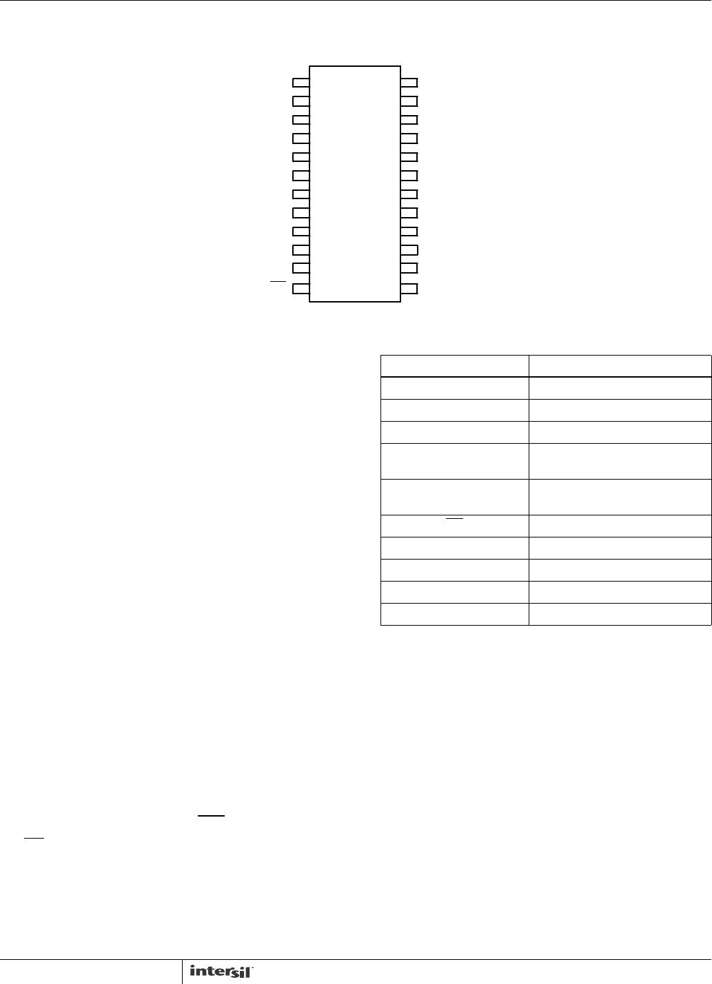
Block Diagram
INTERFACE
AND
CONTROL
CIRCUITRY
SCL
SDA
A0
A1
A2
A3
R
0
R
1
R
2
R
3
WIPER
COUNTER
REGISTER
(WCR)
RESISTOR
ARRAY
POT 1
V
H1
/R
H1
V
L1
/R
L1
R
0
R
1
R
2
R
3
WIPER
COUNTER
REGISTER
(WCR)
V
H0
/R
H0
V
L0
/R
L0
DATA
8
V
W0
/R
W0
V
W1
/R
W1
R
0
R
1
R
2
R
3
RESISTOR
ARRAY
V
H2
/R
H2
V
L2
/R
L2
V
W2
/R
W2
R
0
R
1
R
2
R
3
RESISTOR
ARRAY
V
H3
/R
H3
V
L3
/R
L3
V
W3
/R
W3
WIPER
COUNTER
REGISTER
(WCR)
WIPER
COUNTER
REGISTER
(WCR)
POT 3
POT 2
WP
POT 0
V
CC
V
SS
V+
V-
CAUTION: These devices are sensitive to electrostatic discharge; follow proper IC Handling Procedures.
1-888-INTERSIL or 1-888-468-3774
| Copyright Intersil Americas Inc. 2005, 2006, 2011. All Rights Reserved
Intersil (and design) and XDCP are trademarks owned by Intersil Corporation or one of its subsidiaries.
All other trademarks mentioned are the property of their respective owners.
Data Sheet FN8168.6December 15, 2011