13
FN8168.6
December 15, 2011
Power-Up and Power-Down Requirement
The are no restrictions on the sequencing of the bias supplies
V
CC
, V+, and V- provided that all three supplies reach their final
values within 1ms of each other. At all times, the voltages on
the potentiometer pins must be less than V+ and more than V-.
The recall of the wiper position from nonvolatile memory is not
in effect until all supplies reach their final value. The V
CC
ramp
rate specification is always in effect.
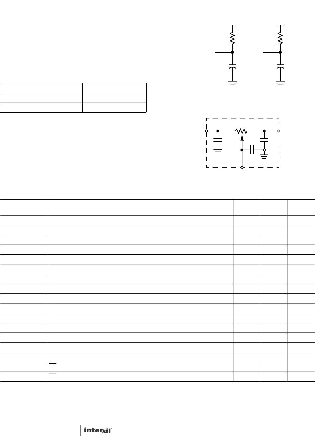
Equivalent AC Load Circuit
Test Circuit #3 SPICE Macro Model
AC Test Conditions
Input Pulse Levels V
CC
x 0.1 to V
CC
x 0.9
Input Rise and Fall Times 10ns
Input and Output Timing Level V
CC
x 0.5
5V
1533Ω
100pF
SDA OUTPUT
2.7V
100pF
10pF
R
H
R
TOTAL
C
H
25pF
C
W
C
L
10pF
R
W
R
L
MACRO MODEL
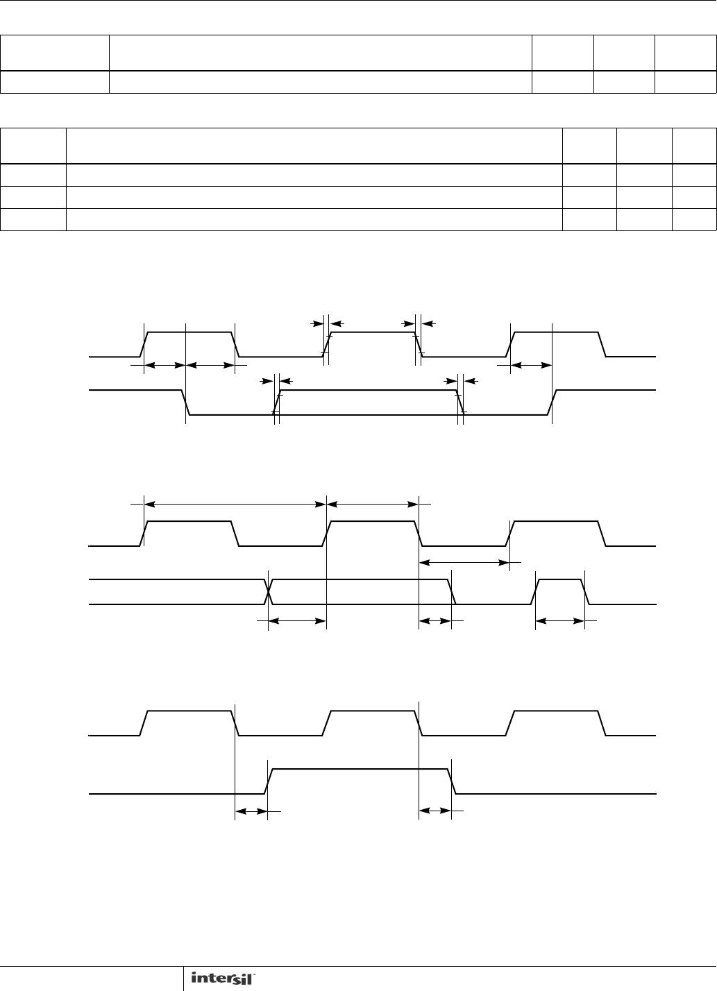
AC Timing Over recommended operating conditions, unless otherwise specified.
SYMBOL PARAMETER
MIN
(Note 12)
MAX
(Note 12) UNIT
f
SCL
Clock Frequency 400 kHz
t
CYC
Clock Cycle Time 2500 ns
t
HIGH
Clock High Time 600 ns
t
LOW
Clock Low Time 1300 ns
t
SU:STA
Start Setup Time 600 ns
t
HD:STA
Start Hold Time 600 ns
t
SU:STO
Stop Setup Time 600 ns
t
SU:DAT
SDA Data Input Setup Time 100 ns
t
HD:DAT
SDA Data Input Hold Time 30 ns
t
R
SCL and SDA Rise Time (Note 20) 300 ns
t
F
SCL and SDA Fall Time (Note 20) 300 ns
t
AA
SCL Low to SDA Data Output Valid Time 900 ns
t
DH
SDA Data Output Hold Time 50 ns
T
I
Noise Suppression Time Constant at SCL and SDA Inputs 50 ns
t
BUF
Bus Free Time (Prior to any Transmission) 1300 ns
t
SU:WPA
WP, A0, A1, A2 and A3 Setup Time 0 ns
t
HD:WPA
WP, A0, A1, A2 and A3 Hold Time 0 ns
NOTE:
20. A device must internally provide a hold time of at least 300ns for the SDA signal in order to bridge the undefined region of the falling edge of SCL.
X9258