Expand menu
Hello, Sign in
My Account
0
Cart
Home
Products
Sensors
Semiconductors
Passive Components
Connectors
Power
Electromechanical
Optoelectronics
Circuit Protection
Integrated Circuits - ICs
Main Products
Manufacturers
Blog
Services
About OMO
About Us
Contact Us
Check Stock
410-251-B
P1-P3
P4-P6
P7-P9
P10-P12
JTAG -SMT2
™
Program
ming Mod
ule for Xilinx® FPGAs
Copyright Digilent, Inc. All
rights reserved.
Other product and com
pany names me
ntioned may be tra
demarks of their res
pective owners.
Page
10
of
12
6
A
b
s
o
l
u
t
e
M
a
x
i
m
u
m
R
a
t
i
n
g
s
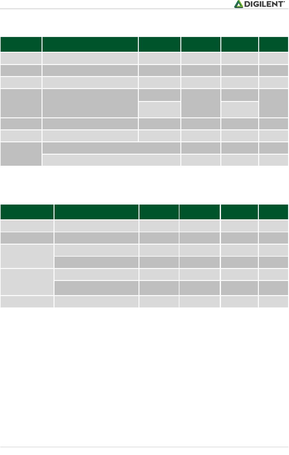
Symbol
Parameter
Condition
Min
Max
Unit
Vdd
Operating supply voltage
-0.3
4.0
V
Vref
I/O reference/supply voltag
e
-0.3
6
V
VIO
Signal Voltage
-0.3
6
V
I
IK
,I
OK
TMS, TCK, TDI, TDO,
GPIO0, GPIO1,
GPIO2
DC Input/Outpu
t Diode Current
VIO < -0.3V
-
50
mA
VIO > 6V
+20
I
OUT
DC Output Current
±50
mA
T
STG
Storage Temperature
-10
+
60
ºC
ESD
Human Body Mod
el JESD22-A
114
4
000
V
Charge Device Model JESD2
2-C101
2
00
0
V
7
D
C
O
p
e
r
a
t
i
n
g
C
h
a
r
a
c
t
e
r
i
s
t
i
c
s
Symbol
Parameter
Min
Typ
Max
Unit
Vdd
Operating supply voltage
2.97
3.3
3.63
Volts
Vref
I/O reference/supply voltag
e
1.65
2.5/3.3
5.5
Volts
TDO, GPIO0,
GPIO1, GPIO2
Input High Volt
age (V
IH
)
1.62
5.5
Volts
Input Low Voltage (V
IL
)
0
0.65
Volts
TMS, TCK, TDI,
GPIO0, GPIO1,
GPIO2
Output High
(V
OH
)
0.85 x Vref
0.95 x Vref
Vref
Volts
Output Low (V
OL
)
0
0.05 x Vref
0.15 x Vref
Volts
T
A
Operating Temperature
-
40
-
85
ºC
JTAG -SMT2
™
Program
ming Mod
ule for Xilinx® FPGAs
Copyright Digilent, Inc. All
rights reserved.
Other product and com
pany names me
ntioned may be tra
demarks of their res
pective owners.
Page
11
of
12
8
A
C
O
p
e
r
a
t
i
n
g
C
h
a
r
a
c
t
e
r
i
s
t
i
c
s
The JTAG-
SMT2’s JTA
G signals operate accord
ing to the timi
ng diagram in Fig. 12.
The SMT2 supports
JTAG/TCK
frequencies from 30 MHz to 8
KHz at in
teger divisions of 30
MHz from 1 to 3750. Co
mmon frequencie
s include 30
MHz, 15 MHz, 10 Mh
z, 7.5 MHz, an
d 6 MH
z (see Table 2). The JTAG/TC
K operating frequency
can be set within the
Xilinx Tools.
No
te: P
lease refer to Xilinx’s iMPA
CT documen
tation for more informatio
n.
TDI
TCK
TDO
T
CKH
T
CKL
T
CK
T
CD_TDI
T
HD
T
SETUP
TMS
T
CD_TMS
9
M
o
u
n
t
i
n
g
t
o
H
o
s
t
P
C
B
s
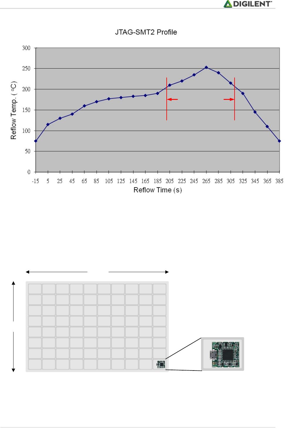
The JTAG-SMT2 modu
le has a
moisture sensiti
vity level (MSL) o
f 3
.
It is suitabl
e for reflow for
up to 168 hou
rs
without addition
al drying.
The factory finishes the J
TAG-SMT2
signal
pads with th
e ENIG pro
cess using 2u” go
ld over 150u” electro
less nickel.
This makes the SMT2 compat
ible with mo
st mounting and r
eflow processes (see Fig. 1
3). The bind
ing force o
f the
solder is sufficient to h
old the SMT2 firmly in place
so mountin
g should r
equ
ire no additional
adhesives.
Symbol
Parameter
Min
Max
T
CK
T
CK
period
30
ns
125µs
T
CKH
, T
CKL
T
CLK
pulse width
15ns
62.5µs
T
CD
_TMS
T
CLK
to TMS
-0
.5
ns
12.
35
ns
T
CD
_TDI
T
CLK
to TDI
-0
.5
ns
8.
15
ns
T
SETUP
TDO Setup time
15.8
ns
T
HD
TDO Hold time
0
ns
Figure 12. Timin
g diag
ram.
Figure 12. Timin
g diag
ram.
Noteoajf
ojeafa
Note
Table 2. JTAG sig
nal timin
g.
Note: these
parameters a
re specified for Vref
= 3.3V.
JTAG -SMT2
™
Program
ming Mod
ule for Xilinx® FPGAs
Copyright Digilent, Inc. All
rights reserved.
Other product and com
pany names me
ntioned may be tra
demarks of their res
pective owners.
Page
12
of
12
Limit time above
205°C to less
than 110s
10
P
a
c
k
a
g
i
n
g
Digilent ships small quan
tities of less than
45
p
er order individually packaged
in antistatic bags. Digil
ent will pack
and ship larger qu
antities in groups of
45
positioned in a
n antistatic bu
bble tray (see Fig.
14).
35cm
28cm
Figure 13. JTAG-SM
T2 reflow temper
ature over time.
Figure 14. JTAG-SM
T2 shippin
g arrangement.
P1-P3
P4-P6
P7-P9
P10-P12
410-251-B
Mfr. #:
Buy 410-251-B
Manufacturer:
Digilent
Description:
Hardware Debuggers JTAG-SMT2, tray
Lifecycle:
New from this manufacturer.
Delivery:
DHL
FedEx
Ups
TNT
EMS
Payment:
T/T
Paypal
Visa
MoneyGram
Western
Union
Products related to this Datasheet
410-251-B