Expand menu
Hello, Sign in
My Account
0
Cart
Home
Products
Sensors
Semiconductors
Passive Components
Connectors
Power
Electromechanical
Optoelectronics
Circuit Protection
Integrated Circuits - ICs
Main Products
Manufacturers
Blog
Services
About OMO
About Us
Contact Us
Check Stock
410-251-B
P1-P3
P4-P6
P7-P9
P10-P12
JTAG -SMT2
™
Program
ming Mod
ule for Xilinx® FPGAs
Copyright Digilent, Inc. All
rights reserved.
Other product and com
pany names me
ntioned may be tra
demarks of their res
pective owners.
Page
7
of
12
E
x
a
m
p
l
e
2
:
I
n
t
e
r
f
a
c
i
n
g
a
Z
y
n
q
-
7
0
0
0
t
h
a
t
u
s
e
s
d
i
f
f
e
r
e
n
t
v
o
l
t
a
g
e
s
f
o
r
V
C
C
O
_
0
a
n
d
V
C
C
O
_
M
I
O
1
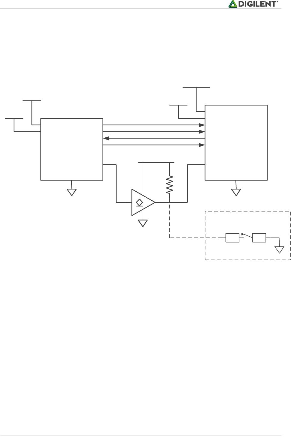
Figure 10 demonstrat
es how to conn
ect the JTAG
-
SMT2 to Xilinx’s Zynq
-7000 silicon
when different voltage
s
supply the VCCO_0 (Progra
mmabl
e Logic Bank 0 Po
wer Supply
) and VCCO_MIO1 (Proce
ssor MIO Bank 1 Power
Supply). If the Zyn
q’s JTAG pins are operating at
a different
voltage than the PS_SRS
T_B, it requires an external
buffer to adjust the le
vel of the GPIO2 signal. Th
e example i
n Fig. 10
demonstrates th
e use of an
open drain b
uffer
to allow for the possib
ility of adding a r
eset button.
VCCO_0
VCCO_MIO1
PS_SRST_B
ZYNQ-
7000
TDO
TMS
TDI
TCK
GND
VDD
VREF
TDO
JTAG-
SMT2
GND
TMS
TDI
TCK
GPIO0
GPIO1
GPIO2
VCCO_0
VCCO_MIO1
3.3V
VCCO_0
VCCO_MIO1
10K
Optional Reset
Button
Figure 10. Use of
an open
drain buffer.
JTAG -SMT2
™
Program
ming Mod
ule for Xilinx® FPGAs
Copyright Digilent, Inc. All
rights reserved.
Other product and com
pany names me
ntioned may be tra
demarks of their res
pective owners.
Page
8
of
12
E
x
a
m
p
l
e
3
:
I
n
t
e
r
f
a
c
i
n
g
a
Z
y
n
q
-
7
0
0
0
w
h
i
l
e
r
e
t
a
i
n
i
n
g
t
h
e
X
i
l
i
n
x
J
T
A
G
H
e
a
d
e
r
Figure 11 below demon
strates how to conn
ect the JTAG
-
SMT2 to Xilinx’
s Zynq
-
7000 silicon alon
gside Xilinx’s 14
-pin
JTAG header. In this exampl
e the open dra
in buffers allow both
the SMT2 and Xilinx JTAG
Header to drive the
PS_SRST_B pin, which may
operate a differ
ent voltage th
an the Zynq
’s JTAG pins.
VCCO_0
VCCO_MIO1
PS_SRST_B
ZYNQ-
7000
TDO
TMS
TDI
TCK
GND
VDD
VREF
TDO
JTAG-
SMT2
GND
TMS
TDI
TCK
GPIO0
GPIO1
GPIO2
VCCO_0
VCCO_MIO1
3.3V
VCCO_0
VCCO_MIO1
10K
Optional Reset
Button
VCCO_MIO1
10K
VCCO_0
VCCO_0
100
100
100
50
Xilinx JTAG
Header
1
2
3
4
5
6
7
8
9
10
11
12
13
14
Jumper
Figure 11. Open d
rain buffers allowing th
e SMT2 and
JTAG Header to drive t
he PS_SRST_B
pin.
JTAG -SMT2
™
Program
ming Mod
ule for Xilinx® FPGAs
Copyright Digilent, Inc. All
rights reserved.
Other product and com
pany names me
ntioned may be tra
demarks of their res
pective owners.
Page
9
of
12
5
M
e
c
h
a
n
i
c
a
l
I
n
f
o
r
m
a
t
i
o
n
11
10
9
1
2
3
4
22
.
75
mm
21
.5
mm
3
mm
5
mm
2
mm
4
mm
Pad
s
on bot
t
o
m
PCB surface
8
6
5
5
mm
2
mm
5.
75
mm
7
SMT
2
Top
Vie
w
Note: PCB di
mensions have a
tolerance of +
/- 0.13mm.
2
3
4
1
9
8
10
11
3.5
mm
3.0
mm
5
mm
4
mm
19
.5
mm
PCB Edge
Rec
om
mend
ed
PCB L
an
d
Pat
te
rn
15
mm
5
21
.
75
mm
6
7
3.0
mm
3.5
mm
4.
75
mm
5
mm
2.6
mm
2.2
mm
6.2
mm
2.6
mm
2.2
mm
6.2
mm
Electrical
Keepout
2.
45
mm
Electrical
Kee
pout
P1-P3
P4-P6
P7-P9
P10-P12
410-251-B
Mfr. #:
Buy 410-251-B
Manufacturer:
Digilent
Description:
Hardware Debuggers JTAG-SMT2, tray
Lifecycle:
New from this manufacturer.
Delivery:
DHL
FedEx
Ups
TNT
EMS
Payment:
T/T
Paypal
Visa
MoneyGram
Western
Union
Products related to this Datasheet
410-251-B