JTAG -SMT2Programming Module for Xilinx® FPGAs
Copyright Digilent, Inc. All rights reserved.
Other product and company names mentioned may be trademarks of their respective owners.
Page 4 of 12
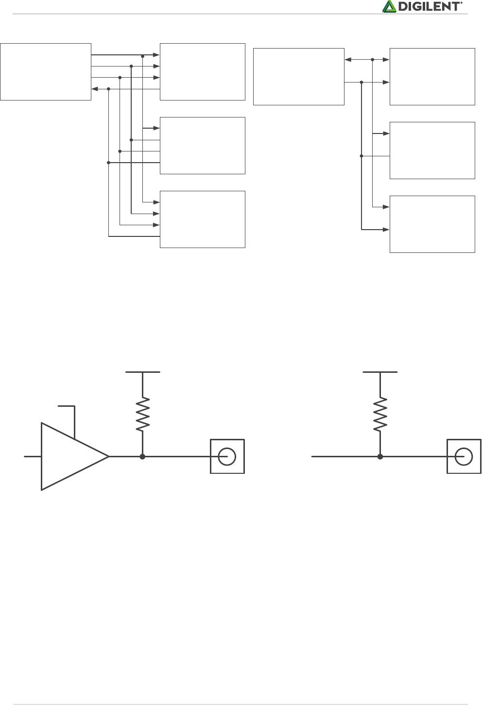
The IEEE 1149.7-2009 specification requires any device that functions as a debug and test system (DTS) to provide
a pull-up bias on the TMS and TDO pins. In order to meet this requirement, the JTAG-SMT2 features weak pull-ups
(100K ohm) on the TMS, TDI, TDO, and TCK signals. Though not required in the specifications, the pull-ups on the
TDI and TCK signals ensure that neither signal floats while another source is not driving them (see Fig. 5).
VREF
Output Pin
(TMS, TDI, TCK)
100K
JtagEN
VREF
Input Pin
(TDO)
100K
Users should place a current limiting resistor between the TMS pin of the SMT2 and the TMSC pin of the TS when
using the JTAG-SMT2 to interface with an 1149.7 compatible TS. If a drive conflict occurs, this resistor should
prevent damage to components by limiting the amount of current flowing between the pins of each device. A 200
ohm resistor will limit the maximum current to 16.5mA when using a 3.3V reference (see Figs. 6 & 7). While this
level of resistance should be sufficient for most applications, the value of the resistor may need to be adjusted to
meet the requirements of the TS.
In most cases users can avoid a drive conflict by having applications that use the SMT2 communicate with the TS in
two-wire mode. Use the applications to reconfigure the TS to use the JScan0, JScan1, JScan2, or JScan3 scan
format prior to disabling the SMT2’s JTAG port.
TMSC
TDIC
TCKC
TDOC
Target
System 0
Target
System 1
Target
System N
4-Wire Star Topology
TMSC
TDIC
TCKC
TDOC
TMSC
TDIC
TCKC
TDOC
TMS
TDI
TCK
TDO
Host
+
JTAG-SMT2
(DTS)
Figure 4. 4-Wire and 2-Wire star topology.
Figure 5. Pull-ups on TMS, TDI, TDO, and TCK signals.
2-Wire Star Topology
TMSC
TDIC
TCKC
TDOC
Target
System 0
Target
System 1
Target
System N
TMSC
TDIC
TCKC
TDOC
TMSC
TDIC
TCKC
TDOC
TMS
TDI
TCK
TDO
Host
+
JTAG-SMT2
(DTS)
JTAG -SMT2Programming Module for Xilinx® FPGAs
Copyright Digilent, Inc. All rights reserved.
Other product and company names mentioned may be trademarks of their respective owners.
Page 5 of 12
VIO
1149.7
Target
System
TDOC
TMSC
TDIC
TCKC
GND
VDD
VREF
TDO
JTAG-
SMT2
GND
TMS
TDI
TCK
VIO
3.3V
VIO
200
VIO
1149.7
Target
System
TDOC
TMSC
TDIC
TCKC
GND
VDD
VREF
TDO
JTAG-
SMT2
GND
TMS
TDI
TCK
VIO
3.3V
VIO
200
The Adept SDK provides an example application that demonstrates how to communicate with a Class T4 TAP
controller using the MScan, OScan0, and OScan1 scan formats.
3 GPIO Pins
The JTAG-SMT2 has three general purpose IO pins (GPIO0, GPIO1, and GPIO2) that are useful for a variety of
different applications. Each pin features high speed, three-state input and output buffers. At power up, the JTAG-
SMT2 disables these output buffers and places the signals in a high-impedance state. Each signal remains in a
high-impedance state until a host application enables DPIO port 0 and configures the applicable pin as an output.
When the host application disables DPIO port 0, all GPIO pins revert to a high-impedance state. Weak pull-ups
(100K ohm) ensure that the GPIO signals do not float while not being actively driven (see Fig. 8).
IO Pin
(GPIO0, GPIO1, GPIO2)
100K
VREF
OEGPIOx
Figure 6. Adding a current limiting resistor.
Figure 7. 200 Ohm resistor limiting current flow.
Figure 8. GPIO signals.
JTAG -SMT2Programming Module for Xilinx® FPGAs
Copyright Digilent, Inc. All rights reserved.
Other product and company names mentioned may be trademarks of their respective owners.
Page 6 of 12
When customers use the JTAG-SMT2 to interface the scan chain of Xilinx’s Zynq platform, they should connect the
GPIO2 pin of the SMT2 to the Zynq’s PS_SRST_B pin. This connection allows the Xilinx Tools to reset the Zynq’s
processor core at various times during debugging operations. Please see the following “Application Examples”
section for more information.
Note: The Xilinx tools expect GPIO2 to be connected to the SRST_B pin on a Zynq chip. As a result, GPIO2 may not be
used as a general purpose I/O if the Xilinx Tools are going to be used to communicate with the SMT2.
Note: DPIO port 0 can only be used while both JTAG and SPI are disabled.
4 Application Examples
Example 1:
Interfacing a Zynq-7000 when VCCO_0 and VCCO_MIO1 use a common supply
Figure 9demonstrates how to connect the JTAG-SMT2 to Xilinx’s Zynq-7000 silicon when the same voltage supplies
both the VCCO_0 (Programmable Logic Bank 0 Power Supply) and the VCCO_MIO1 (Processor MIO Bank 1 Power
Supply).
In this case the SMT2 has a 100K pull-up to VREF, which operates at the same voltage as VCCO_MIO1. This similar
voltage makes it possible to eliminate the external pull-up that is normally required for the PS_SRST_B pin.
VCCO_0
VCCO_MIO1
PS_SRST_B
ZYNQ-
7000
TDO
TMS
TDI
TCK
GND
VDD
VREF
TDO
JTAG-
SMT2
GND
TMS
TDI
TCK
GPIO0
GPIO1
GPIO2
VCCO
3.3V
VCCO
Figure 9. Connecting the JTAG-SMT2 to Xilinx’s Zynq-7000.

410-251-B

Mfr. #:
Manufacturer:
Digilent
Description:
Hardware Debuggers JTAG-SMT2, tray
Lifecycle:
New from this manufacturer.
Delivery:
DHL FedEx Ups TNT EMS
Payment:
T/T Paypal Visa MoneyGram Western Union

Products related to this Datasheet