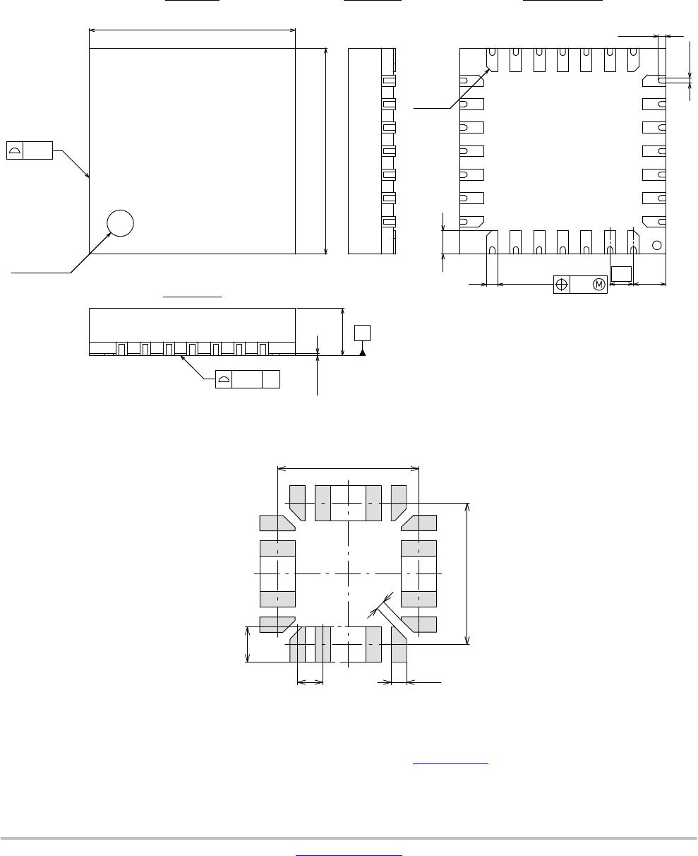
LC717A00AR
www.onsemi.com
10
Table 8. PIN FUNCTION (continued)
Pin Name Pin TypePin FunctionsI/O
SA/SO I/O Slave address selection (I
2
C) /
Data output (SPI)
V
DD
Power supply (2.6 V to 5.5 V) (Note 13)
V
SS
Ground (Earth) (Notes 13, 14)
13.Inserting a high-valued capacitor and a low-valued capacitor in parallel between V
DD
and V
SS
is recommended. In this case, the small-valued
capacitor should be at least 0.1 mF, and is mounted near the LSI.
14.When V
SS
terminal is not grounded in battery-powered mobile equipment, detection sensitivity may be degraded.
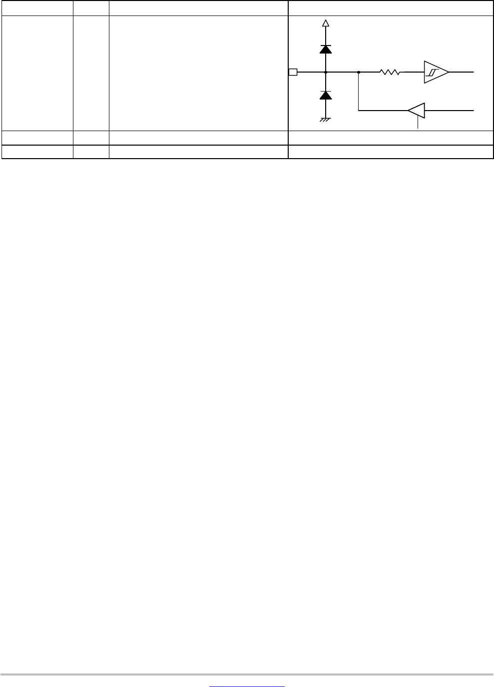
Details of Pin Functions
Cin0 to Cin7
These are the capacitance-sensor-input pins. These pins
are used by connecting them to the touch switch pattern. Cin
and the Cdrv wire patterns should be close to each other. By
doing so, Cdrv and Cin patterns are capacitively coupled.
Therefore, LSI can detect capacitance change near each
pattern as 8-bit digital data.
However, if the shape of each pattern or the capacitively
coupled value of Cdrv is not appropriate, it may not be able
to detect the capacitance change correctly.
In this LSI, there is a two-stage amplifier that detects the
changes in the capacitance and outputs analog-amplitude
values. Cin0 to Cin7 are connected to the inverting input of
the 1
st
amplifier in the LSI.
During measurement process, channels other than the one
being measured are all in “Low” condition.
Leave the unused terminals open.
Cref
It is the reference-capacitance-input pin. It is used by
connecting to the wire pattern like Cin pins or is used by
connecting any capacitance between this pin and Cdrv pin.
In this LSI, there is a two-stage amplifier that detects the
changes in the capacitance and outputs analog-amplitude
values. Cref is connected to the non-inverting input of the 1
st
amplifier in the LSI.
Due to the parasitic capacitance generated in the wire
connections of Cin pins and their patterns, as well as the one
generated between the wire patterns of Cin and Cdrv pins,
Cref may not detect capacitance change of each Cin pin
accurately. In this case, connect an appropriate capacitance
between Cref and Cdrv to detect capacitance change
accurately.
However, if the difference between the parasitic
capacitance of each Cin pin is extremely large, it may not
detect capacitance change in each Cin pin correctly.
Pout0 to Pout7
These are the detection-result-output pins. The
capacitance detection results of Cin0 to Cin7 are compared
with the threshold of the LSI. The pin outputs a “High” or
a “Low” depending on the result.
ERROR
It is the error-occurrence-status-output pin. It outputs
“Low” during normal operation. If there is a calibration error
or a system error, it outputs “High” to indicate that an error
occurred.
Cdrv
It is the output pin for capacitance sensors drive. It outputs
the pulse voltage which is needed to detect capacitance at
Cin0 to Cin7.
Cdrv and Cin wire patterns should be close to each other
so that they are capacitively coupled.
INTOUT
It is the interrupt-output pin. It outputs “High” when
a measurement process is completed.
Connect to a main microcomputer if necessary, and use as
interrupt signal.
Leave the terminal open if not in used.
SCL/SCK
Clock input (I
2
C)/Clock input (SPI). It is the clock input
pin of the I
2
C compatible bus or the SPI depending on the
mode of operation.
If interface is not to be used, fix the pin to “High”.
However, even if interface is not to be used, providing
a communication terminal on board is still recommended.