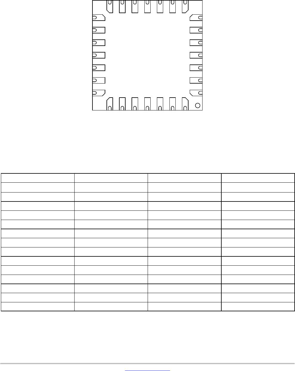
LC717A00AR
www.onsemi.com
7
Block Diagram
Figure 8. Block Diagram
Cin0
SCL/SCK
SDA/SI
V
DD
V
SS
INTOUT
Cin1
Cin2
Cin3
Cin4
Cin5
Cin6
Cin7
Pout0
Pout1
Pout6
Pout7
Pout5
Pout4
Pout3
Pout2
nCS
SA/SO
Cdrv
GAIN
nRST
ERROR
Cref
MUX
1st
AMP
A/D
CONVERTER
2nd
AMP
POR
CONTROL
LOGIC
OSCILLATOR
I
2
C/SPI
+
+
LC717A00AR is capacitance-digital-converter LSI
capable of detecting changes in capacitance in the femto
Farad order. It consists of an oscillation circuit that generates
the system clock, a power-on reset circuit that resets the
system when the power is turned on, a multiplexer that
selects the input channels, a two-stage amplifier that detects
the changes in the capacitance and outputs analog-amplitude
values, a A/D converter that converts the analog-amplitude
values into digital data, and a control logic that controls the
entire chip. Also, it has an I
2
C compatible bus or SPI that
enables serial communication with external devices as
necessary.
LC717A00AR
www.onsemi.com
8
Pin Assignment
Figure 9. Pin Assignment
28 nRSTCin5 8
27 nCSCin6 9
26 SA/SOCin7 10
25 SDA/SIPout0 11
24 SCL/SCKPout1 12
23 GAINPout2 13
22 INTOUTPout3 14
15 Pout4Cin4 7
16 Pout5V
SS
6
17 Pout6V
DD
5
18 Pout7Cin3 4
19 CrefCin2 3
20 ERRORCin1 2
21 CdrvCin0 1
Table 7. PIN ASSIGNMENT
Pin No.
Pin Name Pin No. Pin Name
1 Cin0 15 Pout4
2 Cin1 16 Pout5
3 Cin2 17 Pout6
4 Cin3 18 Pout7
5 V
DD
19 Cref
6 V
SS
20 ERROR
7 Cin4 21 Cdrv
8 Cin5 22 INTOUT
9 Cin6 23 GAIN
10 Cin7 24 SCL/SCK
11 Pout0 25 SDA/SI
12 Pout1 26 SA/SO
13 Pout2 27 nCS
14 Pout3 28 nRST
LC717A00AR
www.onsemi.com
9
Table 8. PIN FUNCTION
Pin Name
I/O Pin Functions Pin Type
Cin0 I/O Capacitance sensor input
R
AMP
V
DD
V
SS
Buffer
Cin1 I/O Capacitance sensor input
Cin2 I/O Capacitance sensor input
Cin3 I/O Capacitance sensor input
Cin4 I/O Capacitance sensor input
Cin5 I/O Capacitance sensor input
Cin6 I/O Capacitance sensor input
Cin7 I/O Capacitance sensor input
Cref I/O Reference capacitance input
Pout0 O Cin0 judgment result output
V
DD
V
SS
Buffer
Pout1 O Cin1 judgment result output
Pout2 O Cin2 judgment result output
Pout3 O Cin3 judgment result output
Pout4 O Cin4 judgment result output
Pout5 O Cin5 judgment result output
Pout6 O Cin6 judgment result output
Pout7 O Cin7 judgment result output
ERROR O Error occurrence status output
Cdrv O Output for capacitance sensors drive
INTOUT O Interrupt output
SCL/SCK I Clock input (I
2
C) / Clock input (SPI)
V
DD
V
SS
R
GAIN I Selection pin of the initial value of
gain of the 2nd-amplifier
nCS I Interface selection / Chip select
inverting input (SPI)
nRST I External reset signal inverting input
SDA/SI I/O Data input and output (I
2
C) /
Data input (SPI)
V
DD
V
SS
R

LC717A00AR-NH

Mfr. #:
Manufacturer:
ON Semiconductor
Description:
Capacitive Touch Sensors DISPLAY DEVICE OTHERS
Lifecycle:
New from this manufacturer.
Delivery:
DHL FedEx Ups TNT EMS
Payment:
T/T Paypal Visa MoneyGram Western Union

Products related to this Datasheet