LTC2862A
1
2862af
For more information www.linear.com/LTC2862A
Typical applicaTion
DescripTion
±60V Fault Protected 3V to 5.5V
RS485/RS422 Transceiver
with Level 4 IEC ESD
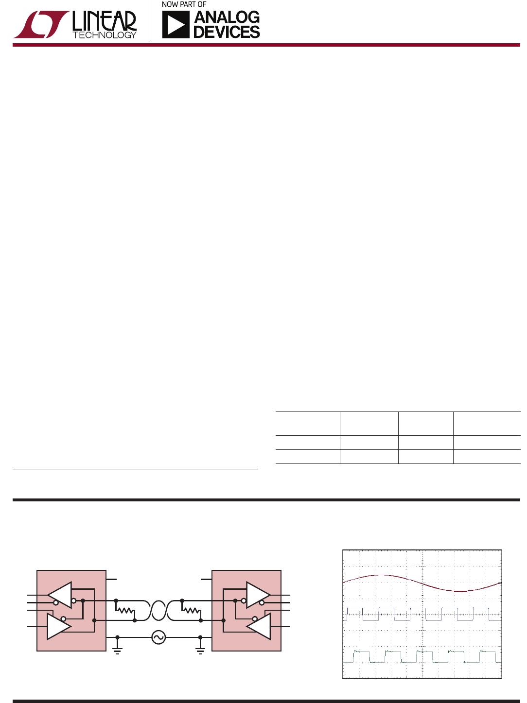
RS485 Link With Large Ground Loop Voltage
FeaTures
applicaTions
n
Protected from Overvoltage Line Faults to ±60V
n
3V to 5.5V Supply Voltage
n
20Mbps or Low EMI 250kbps Data Rate
n
±40kV HBM ESD Interface Pins, ±15kV Other Pins
n
Enhanced Receiver and Failsafe Noise Immunity
n
IEC Level 4 ESD and EFT on Interface Pins
n
Extended Common Mode Range: ±25V
n
Guaranteed Failsafe Receiver Operation
n
High Input Impedance Supports 224 Nodes
n
MP-Grade Option Available (–55°C to 125°C)
n
Fully Balanced Differential Receiver Thresholds for
Low Duty Cycle Distortion
n
Current Limited Drivers and Thermal Shutdown
n
Compliant with TIA/EIA-485-A
n
Pin Compatible with LTC2862 and LT
®
1785
n
Available in DFN and Leaded Packages
n
Supervisory Control and Data Acquisition (SCADA)
n
Industrial Control and Instrumentation Networks
n
Automotive and Transportation Electronics
n
Building Automation, Security Systems and HVAC
n
Medical Equipment
n
Lighting and Sound System Control
LTC2862A-1 Receiving 10Mbps ±200mV Differential
Signal with 1MHz ±25V Common Mode Sweep
PART NUMBER DUPLEX ENABLES
MAX DATA
RATE (bps)
LTC2862A-1 HALF YES 20M
LTC2862A-2 HALF YES 250k
The LT C
®
2862A is a low power, 20Mbps or 250kbps RS485/
RS422 transceiver operating on 3V to 5.5V supplies with
±60V overvoltage fault protection on the interface pins
during all modes of operation, including power-down.
Improvements were made to the LTC2862 for greater ro
-
bustness and signal integrity: ±
40kV
HBM and Level 4 IEC
ESD protection on the interface pins; increased resistance
to electrical overstress; increased receiver noise immunity;
additional receiver noise filtering on the LTC2862A-2; and
an improved failsafe function optimized for high speed in
the LTC2862A-1 and noise rejection in the LTC2862A-2.
Low EMI slew rate limited data transmission is available
in the 250kbps LTC2862A-2 option, while the LTC2862A-1
operates to 20Mbps.
Extended ±25V input common mode range and full fail
-
safe operation improve data communication reliability in
electrically noisy environments
and in the presence of
large ground loop voltages.
L, LT, LTC, LTM, Linear Technology the Linear logo and µModule are registered trademarks of
Analog Devices, Inc.. All other trademarks are the property of their respective owners.
proDucT selecTion GuiDe
GND1
GND2
2862A TA01a
RO1
RE1
DE1
DI1
V
CC1
LTC2862A LTC2862A
V
CC2
RO2
RE2
DE2
DI2
D D
R R
V GROUND LOOP
≤25V PEAK
A,B
50V/DIV
AB
0.5V/DIV
100ns/DIV
2862A TA01b
RO
5V/DIV
RO
A,B
AB
LTC2862A
2
2862af
For more information www.linear.com/LTC2862A
absoluTe MaxiMuM raTinGs
orDer inForMaTion
LEAD FREE FINISH TAPE AND REEL PART MARKING* PACKAGE DESCRIPTION TEMPERATURE RANGE
LTC2862ACS8-1#PBF LTC2862ACS8-1#TRPBF 2862A1 8-Lead (150mil) Plastic SO 0°C to 70°C
LTC2862AIS8-1#PBF LTC2862AIS8-1#TRPBF 2862A1 8-Lead (150mil) Plastic SO –40°C to 85°C
LTC2862AHS8-1#PBF LTC2862AHS8-1#TRPBF 2862A1 8-Lead (150mil) Plastic SO –40°C to 125°C
LTC2862AMPS8-1#PBF LTC2862AMPS8-1#TRPBF 2862A1 8-Lead (150mm) Plastic SO –55°C to 125°C
LTC2862ACS8-2#PBF LTC2862ACS8-2#TRPBF 2862A2 8-Lead (150mil) Plastic SO 0°C to 70°C
LTC2862AIS8-2#PBF LTC2862AIS8-2#TRPBF 2862A2 8-Lead (150mil) Plastic SO –40°C to 85°C
LTC2862AHS8-2#PBF LTC2862AHS8-2#TRPBF 2862A2 8-Lead (150mil) Plastic SO –40°C to 125°C
LTC2862AMPS8-2#PBF LTC2862AMPS8-2#TRPBF 2862A2 8-Lead (150mm) Plastic SO –55°C to 125°C
LTC2862ACDD-1#PBF LTC2862ACDD-1#TRPBF LGYK 8-Lead (3mm × 3mm) Plastic DFN 0°C to 70°C
LTC2862AIDD-1#PBF LTC2862AIDD-1#TRPBF LGYK 8-Lead (3mm × 3mm) Plastic DFN –40°C to 85°C
LTC2862AHDD-1#PBF LTC2862AHDD-1#TRPBF LGYK 8-Lead (3mm × 3mm) Plastic DFN –40°C to 125°C
LTC2862ACDD-2#PBF LTC2862ACDD-2#TRPBF LGYM 8-Lead (3mm × 3mm) Plastic DFN 0°C to 70°C
LTC2862AIDD-2#PBF LTC2862AIDD-2#TRPBF LGYM 8-Lead (3mm × 3mm) Plastic DFN –40°C to 85°C
LTC2862AHDD-2#PBF LTC2862AHDD-2#TRPBF LGYM 8-Lead (3mm × 3mm) Plastic DFN –40°C to 125°C
Consult LTC Marketing for parts specified with wider operating temperature ranges. *The temperature grade is identified by a label on the shipping container.
Consult LTC Marketing for information on non-standard lead based finish parts.
For more information on lead free part marking, go to:
http://www.linear.com/leadfree/
For more information on tape and reel specifications, go to: http://www.linear.com/tapeandreel/
Supply Voltages
V
CC
............................................................. –0.3 to 6V
Logic Input Voltages (RE, DE, DI) .................. 0.3 to 6V
Interface I/O: A, B ..................................... 60V to +60V
Receiver Output (RO) ......................0.3V to (V
CC
+0.3V)
Operating Ambient Temperature Range (Note 4)
LTC2862AC .............................................. 0°C to 70°C
LTC2862AI
...........................................40°C to 85°C
LTC2862A
H ....................................... 40°C to 125°C
LTC2862A
MP ..................................... 55°C to 125°C
Storage Temperature Range .................. 65°C to 150°C
pin conFiGuraTion
LTC2862A-1, LTC2862A-2 LTC2862A-1, LTC2862A-2
1
2
3
4
8
7
6
5
TOP VIEW
V
CC
B
A
GND
RO
RE
DE
DI
S8 PACKAGE
8-LEAD (150mil) PLASTIC SO
T
JMAX
= 150°C, θ
JA
= 120°C/W, θ
JC
= 39°C/W
TOP VIEW
DD PACKAGE
8-LEAD (3mm × 3mm) PLASTIC DFN
EXPOSED PAD (PIN 9) CONNECT TO PCB GND
T
JMAX
= 150°C, θ
JA
= 43°C/W, θ
JC
= 5.5°C/W
5
6
7
8
9
4
3
2
1RO
RE
DE
DI
V
CC
B
A
GND
(Note 1)
http://www.linear.com/product/LTC2862A#orderinfo
LTC2862A
3
2862af
For more information www.linear.com/LTC2862A
elecTrical characTerisTics
SYMBOL PARAMETER CONDITIONS MIN TYP MAX UNITS
Supplies
V
CC
Primary Power Supply
l
3 5.5 V
I
CCS
Supply Current in Shutdown Mode
(C-, I-Grade)
DE = 0V,
RE = V
CC
l
0 10 µA
Supply Current in Shutdown Mode
(H-, MP-Grade)
DE = 0V,
RE = V
CC
l
0 40 µA
I
CCTR
Supply Current with Both Driver and
Receiver Enabled (LTC2862A-1)
No Load, DE = V
CC
, RE = 0V
l
1.1 1.6 mA
I
CCR
Supply Current with Receiver Enabled
(LTC2862A-1)
No Load, DE = RE = 0V
l
1.0 1.4 mA
I
CCTRS
Supply Current with Both Driver and
Receiver Enabled (LTC2862A-2)
No Load, DE = V
CC
, RE = 0V
l
3.5 8 mA
I
CCRS
Supply Current with Receiver Enabled
(LTC2862A-2)
No Load, DE = RE = 0V
l
1.3 1.8 mA
Driver
|V
OD
| Differential Driver Output Voltage R = ∞ (Figure 1)
l
1.5 3 V
CC
V
R = 27Ω (Figure 1)
l
1.5 2 5 V
R = 50Ω (Figure 1)
l
2 2.3 V
CC
V
Δ|V
OD
| Change in Magnitude of Driver Differential
Output Voltage
R = 27Ω or 50Ω (Figure 1)
l
0 0.2 V
V
OC
Driver Common-Mode Output Voltage R = 27Ω or 50Ω (Figure 1)
l
2 3 V
Δ|V
OC
| Change in Magnitude of Driver
Common-Mode Output Voltage
R = 27Ω or 50Ω (Figure 1)
l
0 0.2 V
I
OSD
Maximum Driver Short-Circuit Current –60V ≤ (A or B) ≤ 60V (Figure 2)
l
±150 ±250 mA
Receiver
I
IN
Receiver Input Current (A, B) V
CC
= 0V or 3.3V, V
IN
= 12V (Figure 3)
l
143 µA
V
CC
= 0V or 3.3V, V
IN
= –7V (Figure 3)
l
–100
µA
R
IN
Receiver Input Resistance 0 ≤ V
CC
≤ 5.5V, V
IN
= –25V or 25V (Figure 3) 112
V
CM
Receiver Common Mode Input Voltage
(A + B)/2
l
–25 25 V
V
TH
+
Positive Differential Input Signal Threshold
Voltage (A – B)
–25V ≤ V
CM
≤ 25V
l
125 200 mV
V
TH
Negative Differential Input Signal Threshold
Voltage (A – B)
–25V ≤ V
CM
≤ 25V
l
–200 –125 mV
ΔV
TH
Differential Input Signal Hysteresis
(V
TH
+
– V
TH
)
V
CM
= 0V 250 mV
V
TFS
Differential Input Failsafe Threshold Voltage –25V ≤ V
CM
≤ 25V
l
–200 –75 –10 mV
ΔV
TFS
Differential Input Failsafe Hysteresis
(V
TFS
– V
TH
)
V
CM
= 0V 50 mV
V
OH
Receiver Output High Voltage I(RO) = –3mA (Sourcing)
l
V
CC
0.4V V
CC
0.2V V
V
OL
Receiver Output Low Voltage I(RO) = 3mA (Sinking)
l
0.2 0.4 V
I
OZR
Receiver Three-State (High Impedance)
Output Current on RO
RE = High, V
CC
= 5V, RO = 0V or V
CC
l
–32 5 µA
I
OSR
Receiver Short-Circuit Current RE = Low, RO = 0V or V
CC
l
±20 mA
C
IN
Input Capacitance (A and B) (Note 5) 50 pF
The l denotes the specifications which apply over the full operating
temperature range, otherwise specifications are at T
A
= 25°C. V
CC
= 3.3V unless otherwise noted. (Note 2)

LTC2862AIS8-2#PBF

Mfr. #:
Manufacturer:
Analog Devices Inc.
Description:
RS-422/RS-485 Interface IC 250kbps 60V Fault Protected RS485 Transceiver (Half Duplex + Enables)
Lifecycle:
New from this manufacturer.
Delivery:
DHL FedEx Ups TNT EMS
Payment:
T/T Paypal Visa MoneyGram Western Union