LTC2862A
13
2862af
For more information www.linear.com/LTC2862A
applicaTions inForMaTion
Enhanced EOS Protection
The improved ESD protection of the LTC2862A also pro-
vides superior resistance to electrical overstress (EOS)
damage in the presence of large fault voltages applied from
low impedance faults. The
LTC2862A employs thyristor
type ESD protection on the A, B pins. While thyristors have
the low on-state impedance and high robustness needed
to achieve the very high levels of ESD protection of the
LTC2862A, they have the disadvantage of snapping back
to a low voltage conduction state after they have been
triggered by an initial voltage that exceeds ~±80V. In the
presence of a high voltage, high current fault source, the
large resulting currents will blow the bond wires inside
the LTC2862A package, resulting in a failed chip.
The LTC2862A mitigates the probability of this type of failure
by establishing a very high trigger current in addition to a
higher trigger voltage. In order to trigger the ESD cell, the
fault must not only exceed the ~±80V trigger voltage, but
must be able to source ~±500mA at that voltage to initiate
the snapback of the ESD cell. This makes the LTC2862A
much less susceptible to snapback induced failures created
by high voltage noise spikes or voltage transients caused
by inductive overshoot when the A,B pins are shorted to a
fault voltage source. (The snapback characteristics of the
ESD protection are not tested during production.)
Driver
The driver provides full RS485/RS422 compatibility. When
enabled, if DI is high, A–B is positive. When the driver is
disabled, both transmitter outputs are high impedance,
and the impedance is dominated by the receiver input
resistance, R
IN
.
Driver Overvoltage and Overcurrent Protection
The driver outputs are protected from short circuits to any
voltage within the Absolute Maximum range of –60V to
60V. The maximum current in a fault condition is ±250mA.
The driver includes a progressive foldback current limiting
circuit that continuously reduces the driver current limit
with increasing output fault voltage. The fault current is
less than ±15mA for fault voltages over ±40V.
All devices also feature thermal shutdown protection that
disables the driver and receiver in case of excessive power
dissipation (see Note 4). (Thermal shutdown is not tested
during production.)
Full Failsafe Operation
When the absolute value of the differential voltage between
the A and B pins is greater than 200mV with the receiver
enabled, the state of RO will reflect the polarity of (A–B).
These parts have a failsafe feature that guarantees the
receiver output will be in a logic 1 state (the idle state) when
the inputs are shorted, left open, or terminated but not
driven. The delay allows normal data signals to transition
through the threshold region without being interpreted as
a failsafe condition. This failsafe feature is guaranteed to
work for inputs spanning the entire common mode range
of –25V to 25V.
Most competing devices achieve the failsafe function by a
simple negative offset of the input threshold voltage. This
causes the receiver to interpret a zero differential voltage
as a logic 1 state. The disadvantage of this approach is
the input offset can introduce duty cycle asymmetry at the
receiver output that becomes increasingly worse with low
input signal levels and slow input edge rates.
Other competing devices use internal biasing resistors to
create a positive bias at the receiver inputs in the absence
of an external signal. This type of failsafe biasing is
ineffective if the network lines are shorted, or if the network
is terminated but not driven by an active transmitter.
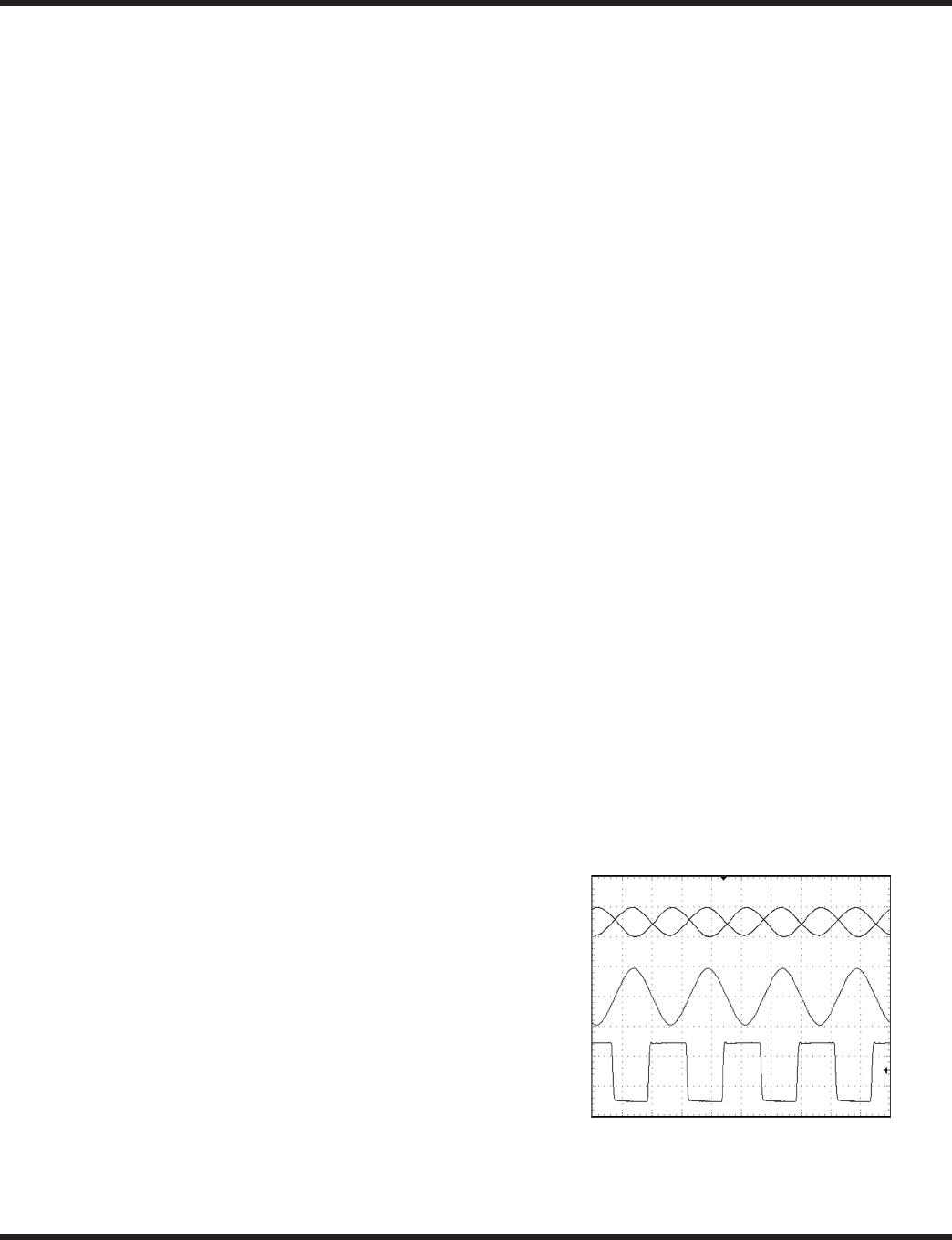
Figure9. Duty Cycle of Balanced Receiver with ±200mV
10Mbps Input Signal
A, B
200mV/DIV
A–B
200mV/DIV
40ns/DIV
286A F08
RO
1.6V/DIV
LTC2862A
14
2862af
For more information www.linear.com/LTC2862A
The LTC2862A uses fully symmetric positive and negative
receiver thresholds V
TH
and V
TH
+
(typically ±125mV) to
maintain good duty cycle symmetry at low signal levels. The
failsafe operation is performed with a window comparator
to determine when the differential input voltage falls above
the V
TFS
failsafe threshold (typically –75mV) but below
the V
TH
+
threshold. If this condition persists for more
than about 40ns for the LTC2862A-1 or 1.2µs for the
LTC2862A-2 the failsafe condition is asserted and the RO
pin is forced to the logic 1 state. This circuit provides full
failsafe operation and a large dynamic signal hysteresis of
~250mV between V
TH
and V
TH
+
with no negative impact
to receiver duty cycle symmetry, as shown in Figure9.
The input signal in Figure9 was obtained by driving a
10Mbps RS485 signal through 1000 feet of cable, thereby
attenuating it to a ±200mV signal with slow rise and fall
times. Good duty cycle symmetry is observed at RO despite
the degraded input signal.
The failsafe circuit has been enhanced with noise filtering
to exit the failsafe state. In the absence of noise filtering, a
noise transient that momentarily forces the A-B differential
voltage below the V
TH
receiver threshold will cause the
RO output to go low, which may be interpreted as a false
start character by the microcontroller. The LTC2862A
receiver reduces these false signals by low pass filtering
the signal to exit the failsafe state. The noise filtering in the
failsafe circuit of the LTC2862A-2 is much greater than in
the LTC2862A-1, commensurate with its lower data rate.
For example, the LTC2862A-1 exits the failsafe state when
a –1V differential pulse of about 3ns duration is applied,
while the LTC2862A-2 requires a –1V pulse of about 400ns
duration to exit the failsafe state. (The minimum pulse
widths to enter or exit the failsafe state are not tested in
production, but the underlying filtering is reflected in the
t
FSN
, t
FSX
, t
FSNS
, and t
FSXS
measurements).
Enhanced Receiver Noise Immunity
An additional benefit of the fully symmetric receiver
thresholds is enhanced receiver noise immunity. The
differential input signal must go above the positive
threshold to register as a logic 1 and go below the
negative threshold to register as a logic 0. This provides
a hysteresis of 250mV (typical) at the receiver inputs for
any valid data signal. (An invalid data condition such as
a DC sweep of the receiver inputs will produce a different
observed hysteresis due to the activation of the failsafe
circuit.) Competing devices that employ a negative offset
of the input threshold voltage generally have a much
smaller hysteresis and subsequently have lower receiver
noise immunity.
The LTC2862A-2 provides additional noise immunity
by adding low-pass filtering to the differential signal in
its receiver. Commensurate with its maximum data rate
of 250kbps, the LTC2862A-2 receiver attenuates high
frequency signals above approximately 660kHz. This low-
pass filter removes high frequency noise transients that
might otherwise be interpreted as data. (High frequency
noise filtering is not tested in production, but the underlying
filtering is reflected in the t
PLHR
, t
PHLR
, t
PLHRS
, and t
PHLRS
measurements).
RS485 Network Biasing
RS485 networks are usually biased with a resistive divider
to generate a differential voltage of ≥200mV on the data
lines, which establishes a logic 1 state (the idle state)
when all the transmitters on the network are disabled. The
values of the biasing resistors are not fixed, but depend
on the number and type of transceivers on the line and
the number and value of terminating resistors. Therefore,
the values of the biasing resistors must be customized
to each specific network installation, and may change if
nodes are added to or removed from the network.
The internal failsafe feature of the LTC2862A eliminates the
need for external network biasing resistors provided they
are used in a network of transceivers with similar internal
failsafe features. The LTC2862A transceivers will operate
correctly on biased, unbiased, or under-biased networks.
Hi-Z State
The receiver output is internally driven high (to V
CC
) or
low (to GND) with no external pull-up needed. When the
receiver is disabled the RO pin becomes Hi-Z with a 250k
pull-up resistor to V
CC
.
applicaTions inForMaTion
LTC2862A
15
2862af
For more information www.linear.com/LTC2862A
High Receiver Input Resistance
The bus receiver input load from A or B to GND is less than
one-seventh unit load, permitting a total of 224 receivers
per system without exceeding the RS485 receiver loading
specification. The input load of the receiver is unaffected by
enabling/disabling the receiver or by powering/unpowering
the part.
Supply Current
The unloaded static supply currents in these devices
are low typically 1.1mA for non slew limited devices
and 3.5mA for slew limited devices. In applications
with resistively terminated cables, the supply current is
dominated by the driver load. For example, when using two
120Ω terminators with a differential driver output voltage
of 2V, the DC load current is 33mA, which is sourced by
the positive voltage supply. Power supply current increases
with toggling data due to capacitive loading and this term
can increase significantly at high data rates. A plot of
the supply current vs data rate is shown in the Typical
Performance Characteristics of this data sheet.
During fault conditions with a positive voltage larger than
the supply voltage applied to the transmitter pins, or during
transmitter operation with a high positive common mode
voltage, positive current of up to 80mA may flow from the
transmitter pins back to V
CC
. If the system power supply
or loading cannot sink this excess current, a 5.6V 1W
1N4734 Zener diode may be placed between V
CC
and GND
to prevent an overvoltage condition on V
CC
.
The LTC2862A contains a supply undervoltage lockout
circuit that enables the transmitter and receiver outputs
when V
CC
exceeds ~2.7V and disables the transmitter and
receiver outputs when V
CC
falls below ~2.5V.
When the LTC2862A is unpowered, the logic inputs (DE,
DI, RE) are high impedance for voltages > 0V. Each input
has a diode clamp to GND that will conduct if a negative
voltage sufficient to forward bias the diode (~ 0.6V at
25°C) is applied to the pad. The RO output contains a CMOS
driver with parasitic diodes to GND and V
CC
. The diode to
GND will conduct if forward biased by a negative voltage
below GND, while the diode to V
CC
will conduct if forward
biased by a positive voltage above V
CC
. If V
CC
is low, this
applicaTions inForMaTion
will result in the RO line being clamped to approximately
0.6V above V
CC
. The impedance of the logic inputs and the
RO output are not tested with the LTC2862A unpowered.
Shutdown Mode Delay
The LTC2862A features a low power shutdown mode
that is entered when both the driver and the receiver
are simultaneously disabled (pin DE low and RE high).
A shutdown mode delay of approximately 250ns (not
tested in production) is imposed after this state is received
before the chip enters shutdown. If either DE goes high
or RE goes low during this delay, the delay timer is reset
and the chip does not enter shutdown. This reduces the
chance of accidentally entering shutdown if DE and RE are
driven in parallel by a slowly changing signal or if DE and
RE are driven by two independent signals with a timing
skew between them.
This shutdown mode delay does not affect the outputs of
the transmitter and receiver, which start to switch to the
high impedance state upon the reception of their respec-
tive disable signals as defined by the parameters t
SHDND
and t
SHDNR
. The shutdown mode delay affects only the
time when all the internal circuits that draw DC power
from V
CC
are turned off.
High Speed Considerations
A ground plane layout with a 0.1µF bypass capacitor placed
less than 7mm away from the V
CC
pin is recommended.
The PC board traces connected to signals A/B should be
symmetrical and as short as possible to maintain good
differential signal integrity. To minimize capacitive effects,
the differential signals should be separated by more than
the width of a trace and should not be routed on top of
each other if they are on different signal planes.
Care should be taken to route outputs away from any
sensitive inputs to reduce feedback effects that might
cause noise, jitter, or even oscillations.
The logic inputs have a typical hysteresis of 100mV to
provide noise immunity. Fast edges on the outputs can
cause glitches in the ground and power supplies which are
exacerbated by capacitive loading. If a logic input is held
near its threshold (typically V
CC
/2), a noise glitch from a
LTC2862AIS8-2#PBF

Mfr. #:
Manufacturer:
Analog Devices Inc.
Description:
RS-422/RS-485 Interface IC 250kbps 60V Fault Protected RS485 Transceiver (Half Duplex + Enables)
Lifecycle:
New from this manufacturer.
Delivery:
DHL FedEx Ups TNT EMS
Payment:
T/T Paypal Visa MoneyGram Western Union