7
LTC3404
3404fb
+
+
+
+
+
OVDET
EA
+
I
RCMP
+
I
COMP
8
7
3
1
RUN
PLL LPF
VCO
X
Y
Y = “0” ONLY WHEN X IS A CONSTANT “1”
BURST
DEFEAT
SLOPE
COMP
OSC
SYNC/MODE
0.6V
FREQ
SHIFT
V
REF
0.8V
0.85V
Ω
g
m
= 0.5m
0.8V REF
SHUTDOWN
0.55V
0.8V
SLEEP
V
IN
V
IN
V
IN
V
IN
I
TH
SLEEP
V
FB
EN
BURST
V
IN
2
S
R
RS LATCH
SWITCHING
LOGIC
AND
BLANKING
CIRCUIT
ANTI-
SHOOT-
THRU
Q
Q
6Ω
6
SW
5
GND
3404 BD
4
P-CHP-CH
N-CH
FU CTIO AL DIAGRA
U
U
W
OPERATIO
U
Main Control Loop
The LTC3404 uses a constant frequency, current mode
step-down architecture. Both the main (P-channel MOS-
FET) and synchronous (N-channel MOSFET) switches are
internal. During normal operation, the internal top power
MOSFET is turned on each clock cycle when the oscillator
sets the RS latch, and turned off when the current com-
parator, I
COMP
, resets the RS latch. The peak inductor
current at which I
COMP
resets the RS latch is controlled by
the voltage on the I
TH
pin, which is the output of error
amplifier EA. The V
FB
pin, described in the Pin Functions
section, allows EA to receive an output feedback voltage
from an external resistive divider. When the load current
increases, it causes a slight decrease in the feedback
voltage, V
FB
, relative to the 0.8V internal reference, which
in turn, causes the I
TH
voltage to increase until the average
inductor current matches the new load current. While the
top MOSFET is off, the bottom MOSFET is turned on until
either the inductor current starts to reverse as indicated by
the current reversal comparator I
RCMP
, or the beginning of
the next clock cycle.
Comparator OVDET guards against transient overshoots
>6.25% by turning the main switch off and keeping it off
until the fault is removed.
Burst Mode Operation
The LTC3404 is capable of Burst Mode operation in which
the internal power MOSFETs operate intermittently based
on load demand. To enable Burst Mode operation, simply
tie the SYNC/MODE pin to V
IN
or connect it to a logic high
(V
SYNC/MODE
> 1.5V). To disable Burst Mode operation and
enable PWM pulse skipping mode, connect the SYNC/
MODE pin to GND. In this mode, the efficiency is lower at
light loads, but becomes comparable to Burst Mode
operation when the output load exceeds 50mA. The ad-
vantage of pulse skipping mode is lower output ripple and
less interference to audio circuitry.
8
LTC3404
3404fb
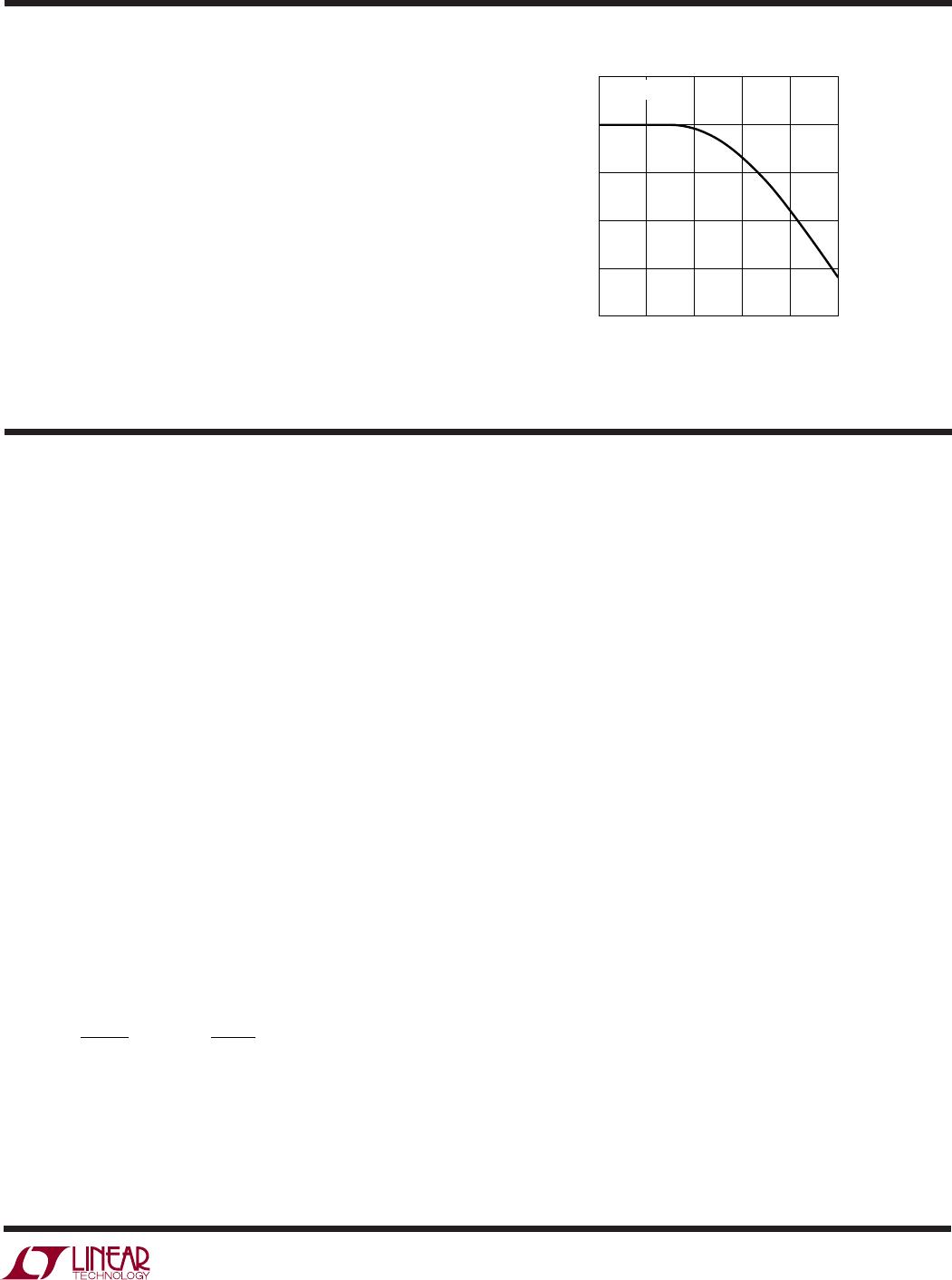
Figure 1. Maximum Output Current vs Input Voltage
SUPPLY VOLTAGE (V)
2.5
MAXIMUM OUTPUT CURRENT (mA)
1200
1000
800
600
400
200
0
3.5 4.5 5.5 6.5
3404 • F01
7.5
L = 4.7μH
V
OUT
= 3.3V
V
OUT
= 2.5V
V
OUT
= 1.5V
OPERATIO
U
When the converter is in Burst Mode operation, the peak
current of the inductor is set to approximately 250mA,
even though the voltage at the I
TH
pin indicates a lower
value. The voltage at the I
TH
pin drops when the inductor’s
average current is greater than the load requirement. As
the I
TH
voltage drops below approximately 0.55V, the
BURST comparator trips, causing the internal sleep line to
go high and forces off both power MOSFETs. The I
TH
pin
is then disconnected from the output of the EA amplifier
and held a diode voltage (0.7V) above ground.
In sleep mode, both power MOSFETs are held off and a
majority of the internal circuitry is partially turned off,
reducing the quiescent current to 10μA. The load current
is now being supplied solely from the output capacitor.
When the output voltage drops, the I
TH
pin reconnects to
the output of the EA amplifier and the top MOSFET is again
turned on and this process repeats.
Short-Circuit Protection
When the output is shorted to ground, the frequency of the
oscillator is reduced to about 200kHz, 1/7 the nominal
frequency. This frequency foldback ensures that the
inductor current has ample time to decay, thereby prevent-
ing runaway. The oscillator’s frequency will progressively
increase to 1.4MHz (or the synchronized frequency) when
V
FB
rises above 0.3V.
Frequency Synchronization
A phase-locked loop (PLL) is available on the LTC3404 to
allow the internal oscillator to be synchronized to an
external source connected to the SYNC/MODE pin. The
output of the phase detector at the PLL LPF pin operates
over a 0V to 2.4V range corresponding to 1MHz to 1.7MHz.
When locked, the PLL aligns the turn-on of the top MOS-
FET to the rising edge of the synchronizing signal.
When the LTC3404 is clocked by an external source, Burst
Mode operation is disabled; the LTC3404 then operates in
PWM pulse skipping mode. In this mode, when the output
load is very low, current comparator I
COMP
may remain
tripped for several cycles and force the main switch to stay
off for the same number of cycles. Increasing the output
load slightly allows constant frequency PWM operation to
resume. This mode exhibits low output ripple as well as
low audio noise and reduced RF interference while provid-
ing reasonable low current efficiency.
Frequency synchronization is inhibited when the feedback
voltage V
FB
is below 0.6V. This prevents the external clock
from interfering with the frequency foldback for short-
circuit protection.
Dropout Operation
When the input supply voltage decreases toward the
output voltage, the duty cycle increases toward the maxi-
mum on-time. Further reduction of the supply voltage
forces the main switch to remain on for more than one
cycle until it reaches 100% duty cycle. The output voltage
will then be determined by the input voltage minus the
voltage drop across the internal P-channel MOSFET and
the inductor.
Low Supply Operation
The LTC3404 is designed to operate down to an input
supply voltage of 2.65V although the maximum allowable
output current is reduced at this low voltage. Figure 1
shows the reduction in the maximum output current as a
function of input voltage for various output voltages.
Another important detail to remember is that at low input
supply voltages, the R
DS(ON)
of the P-channel switch
increases. Therefore, the user should calculate the power
dissipation when the LTC3404 is used at 100% duty cycle
with a low input voltage (see Thermal Considerations in
the Applications Information section).
9
LTC3404
3404fb
Figure 2. Maximum Inductor Peak Current vs Duty Cycle
DUTY CYCLE (%)
0
MAXIMUM INDUCTOR PEAK CURRENT (mA)
1100
1000
900
800
700
600
80
3404 F02
20
40
60
100
V
IN
= 3.3V
OPERATIO
U
APPLICATIO S I FOR ATIO
WUUU
Slope Compensation and Inductor Peak Current
Slope compensation provides stability in constant fre-
quency architectures by preventing subharmonic oscilla-
tions at high duty cycles. It is accomplished internally by
adding a compensating ramp to the inductor current
signal at duty cycles in excess of 40%. As a result, the
maximum inductor peak current is reduced for duty cycles
>40%. This is shown in the decrease of the inductor peak
current as a function of duty cycle graph in Figure 2.
The basic LTC3404 application circuit is shown on the first
page. External component selection is driven by the load
requirement and begins with the selection of L followed by
C
IN
and C
OUT
.
Inductor Value Calculation
The inductor selection will depend on the operating fre-
quency of the LTC3404. The internal nominal frequency is
1.4MHz, but can be externally synchronized from 1MHz to
1.7MHz.
The operating frequency and inductor selection are inter-
related in that higher operating frequencies allow the use
of smaller inductor and capacitor values. However, oper-
ating at a higher frequency generally results in lower
efficiency because of increased internal gate charge losses.
The inductor value has a direct effect on ripple current. The
ripple current ΔI
L
decreases with higher inductance or
frequency and increases with higher V
IN
or V
OUT
.
Δ =
()( )
I
fL
V
V
V
L OUT
OUT
IN
1
1
(1)
Accepting larger values of ΔI
L
allows the use of smaller
inductors, but results in higher output voltage ripple and
greater core losses. A reasonable starting point for setting
ripple current is ΔI
L
= 0.4(I
MAX
).
The inductor value also has an effect on Burst Mode
operation. The transition to low current operation begins
when the inductor current peaks fall to approximately
250mA. Lower inductor values (higher ΔI
L
) will cause this
to occur at lower load currents, which can cause a dip in
efficiency in the upper range of low current operation. In
Burst Mode operation, lower inductance values will cause
the burst frequency to increase.
Inductor Core Selection
Once the value for L is known, the type of inductor must be
selected. High efficiency converters generally cannot
afford the core loss found in low cost powdered iron cores,
forcing the use of more expensive ferrite, molypermalloy,
or Kool Mμ
®
cores. Actual core loss is independent of core
size for a fixed inductor value, but it is very dependent on
inductance selected. As inductance increases, core losses
go down. Unfortunately, increased inductance requires
more turns of wire and therefore copper losses will
increase.
Ferrite designs have very low core losses and are pre-
ferred at high switching frequencies, so design goals can
concentrate on copper loss and preventing saturation.
Ferrite core material saturates “hard,” which means that
inductance collapses abruptly when the peak design cur-
rent is exceeded. This results in an abrupt increase in

LTC3404MPMS8#TRPBF

Mfr. #:
Manufacturer:
Analog Devices / Linear Technology
Description:
Switching Voltage Regulators Military Plastic: 600mA, 1.4MHz Synch Buck Reg
Lifecycle:
New from this manufacturer.
Delivery:
DHL FedEx Ups TNT EMS
Payment:
T/T Paypal Visa MoneyGram Western Union