LT8631
16
8631fa
For more information www.linear.com/LT8631
so source current increases as source voltage drops. This
looks like a negative resistance load to the source and can
cause the source to current limit or latch low under low
source voltage conditions. The EN/UV threshold prevents
the regulator from operating at source voltages where the
problems might occur. This threshold can be adjusted by
setting the values R3 and R4 such that they satisfy the
following equation:
V
EN THRESHOLD
=
R3
R4
+1
•1.19V
where the LT8631 will remain off until V
IN
is above the
EN/UV threshold. Due to the comparator’s hysteresis,
switching will not stop until the input falls slightly below
the threshold voltage.
When operating in Burst Mode operation for light load
currents, the current through the EN/UV resistor network
can easily be greater than the supply current consumed
by the LT8631. Therefore, the EN/UV resistors should be
large to minimize their effect on efficiency at low loads.
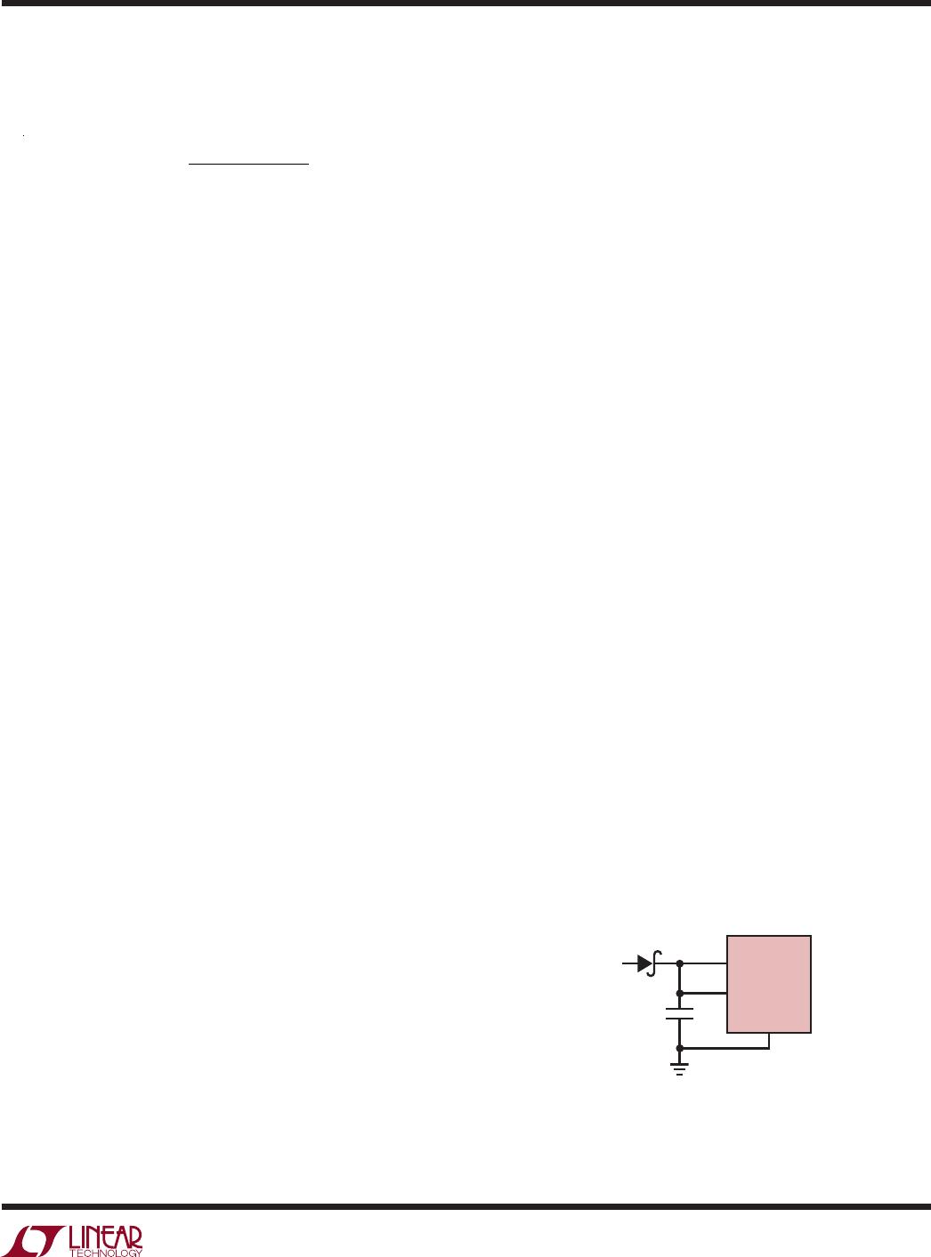
INTV
CC
Regulator
An internal low dropout (LDO) regulator produces the 3V
supply from V
IN
that powers the drivers and the internal
bias circuitry. The INTV
CC
can supply enough current for
the LT8631's circuitry and must be bypassed to ground
with a minimum of 2.2µF ceramic capacitor. Good bypass
-
ing is necessary to supply the high transient currents
required by the power MOSFET gate drivers. To improve
efficiency, the internal regulator draws power from the
V
OUT
pin when the output voltage is 3.5V or higher. If the
V
OUT
pin is below 3.5V, the internal regulator will consume
current from V
IN
. Applications with high input voltage and
high switching frequency where the
internal regulator pulls
current from V
IN
will increase die temperature because of
the higher power dissipation across the regulator. Do not
connect an external load to the INTV
CC
pin.
Soft-Start and Output Voltage Tracking
The LT8631 regulates its output to the lowest voltage
present at either the TR/SS pin or an internal 0.808V
reference. A capacitor from the TR/SS pin to ground is
charged by an internal 4.5µA current source resulting in a
linear output ramp from 0V to the regulated output whose
duration is given by:
T
RAMP
=
TR / SS
4.5µA
At power-up, a reset signal (POR) sets the soft-start latch
and discharges the TR/SS pin with to approximately 0V
to ensure proper start-up. The TR/SS pin has a maximum
current sink capability 230µA. If the TR/SS pin is used to as
a track function for an external voltage, the maximum sink
current must not be exceeded during startup. Exceeding
the maximum TR/SS sink current will inhibit operation.
When the TR/SS pin is fully discharged, the latch is reset
and the internal 4.5µA current source starts to charge the
TR/SS pin. When the TR/SS pin voltage is below ~50mV,
the V
C
pin is pulled low which disables switching.
As the TR/SS pin voltage rises above 50mV, the V
C
pin is
released and the output voltage is regulated to the TR/SS
voltage. When the TR/SS pin voltage exceeds the internal
808mV reference, the output is regulated to the reference.
The TR/SS pin voltage will continue to rise to ~3V.
The soft-start latch is set during several fault conditions:
EN/UV pin is below 1.19V, INTV
CC
has fallen too low, V
IN
is too low, or thermal shutdown. Once the latch is set,
the
TR/SS pin will discharge to ~0V and a new startup
sequence will begin.
If the load exceeds the maximum output switch current,
the output will start to drop causing the internal V
C
clamp
to be activated. As long as the V
C
node is clamped, the TR/
SS pin will be discharged. As a result, the output will be
regulated to the highest voltage that the maximum output
current can support. For example, if the output on the front
page application is loaded by 2Ω the TR/SS pin will drop
to 0.48V, regulating the output at 3V. Once the overload
condition is removed, the output will soft-start from the
temporary voltage level to the normal regulation point.
Since the TR/SS pin is pulled up to the 3V rail and has to
discharge to 0.808V before taking control of regulation,
momentary overload conditions will be tolerated without
APPLICATIONS INFORMATION