LT8631
4
8631fa
For more information www.linear.com/LT8631
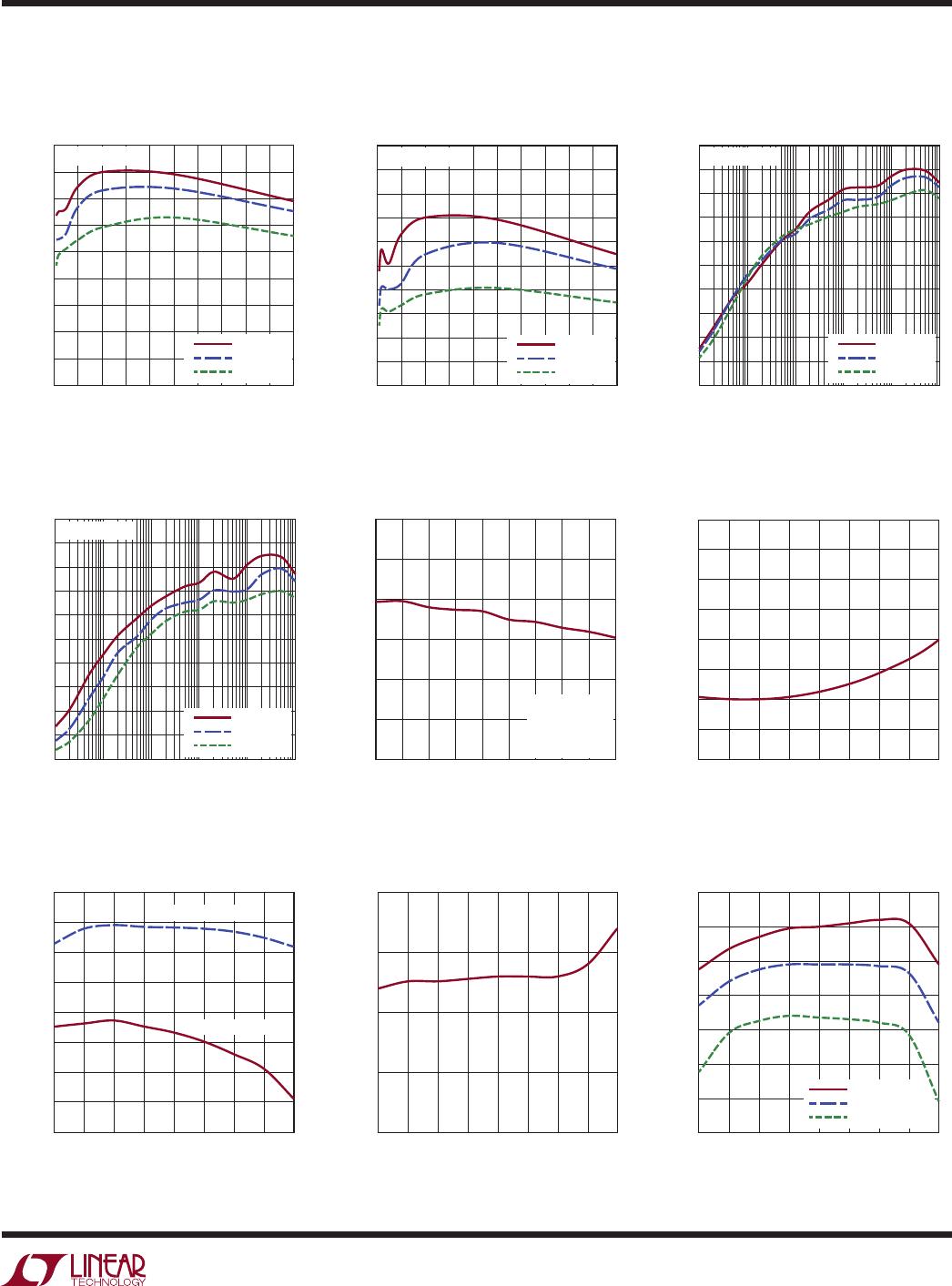
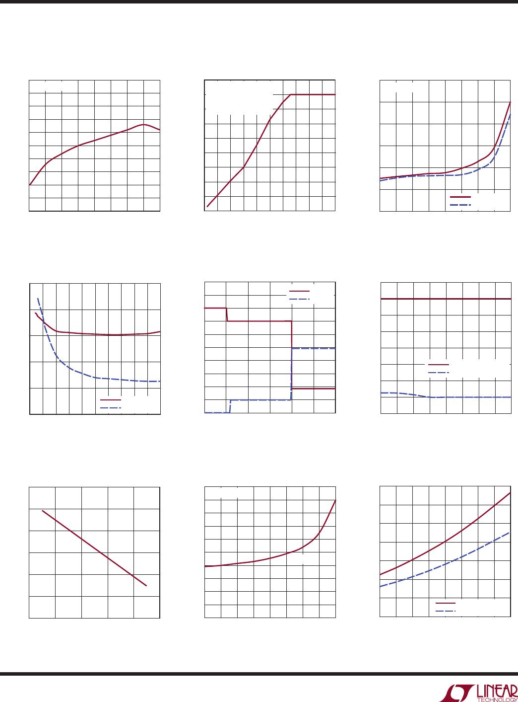
ELECTRICAL CHARACTERISTICS
The l denotes the specifications which apply over the full operating
temperature range, otherwise specifications are at T
J
= 25°C. V
IN
= 15V, V
EN/UV
= 2V, unless otherwise specified. (Note 2)
PARAMETER CONDITIONS MIN TYP MAX UNITS
BST Pin Threshold (Note 8) 2.4 V
SYNC/MODE Pin Current V
SYNC/MODE
= 3V 2 3.4 5.5 µA
SYNC/MODE Threshold 1.0 1.5 2.0 V
Synchronization Range 100 1000 kHz
Note 1: Stresses beyond those listed under Absolute Maximum Ratings
may cause permanent damage to the device. Exposure to any Absolute
Maximum Rating condition for extended periods may affect device
reliability and lifetime.
Note 2: The LT8631EFE is guaranteed to meet performance specifications
from 0°C to 125°C junction temperature. Specifications over the –40°C
to 125°C operating junction temperature range are assured by design,
characterization and correlation with statistical process controls. The
LT8631IFE is guaranteed over the full –40°C to 125°C operating junction
temperature range. The LT8631HFE is guaranteed over the full –40°C to
150°C operating junction temperature range. High junction temperatures
degrade operating lifetimes. Operating lifetime is derated at junction
temperatures greater than 125°C.
Note 3: The LT8631 includes overtemperature protection that is intended
to protect the device during thermal overload conditions. Internal junction
temperature will exceed 150°C when the overtemperature circuitry is
active.
Note 4: An internal power on reset (POR) latch is set on the positive
transition of the EN/UV pin through its threshold or thermal shutdown.
The output of the
latch activates a current source on the TR/SS pin which
typically sinks 230µA while discharging the TR/SS capacitor. The latch is
reset when the TR/SS pin is driven below the soft-start POR threshold or
the EN/UV pin is taken below its threshold.
Note 5:
The threshold is expressed as a percentage of the feedback
reference voltage.
Note 6: The IND to V
OUT
burst current is defined as the maximum value of
current flowing from the IND pin to the V
OUT
during a switch cycle when
operating in Burst Mode.
Note 7: The IND to V
OUT
peak current is defined as the maximum value of
current flowing from the IND pin to the V
OUT
during a switch cycle.
Note 8: The BST pin threshold is defined as the minimum voltage between
the BST and SW pins to keep the top switch on. If the the voltage falls
below the threshold when the top switch is on, a minimum switch off
pulse will be generated.