Data Sheet ADCMP361
APPLICATION INFORMATION
The ADCMP361 is a low power comparator and reference
circuit featuring a 400 mV reference that operates from 1.7 V
to 5.5 V. The comparator is 0.275% accurate with a built-in
hysteresis of 9.3 mV. There are two outputs, one the inverse
of the other. This enables the ADCMP361 to be used as an
inverting or a noninverting comparator circuit. These open-
drain outputs are capable of sinking 40 mA.
COMPARATORS AND INTERNAL REFERENCE
The comparator has one input available externally; the other
comparator input is connected internally to the 400 mV reference.
The rising input threshold voltage of the comparators is designed
to be equal to that of the reference.
POWER SUPPLY
The ADCMP361 is designed to operate from 1.7 V to 5.5 V. A 100 nF
decoupling capacitor is recommended between V
DD
and GND.
INPUTS
The comparator input is limited to the maximum V
DD
voltage
range. The voltage on these inputs can be above V
DD
but never
above the maximum allowed V
DD
voltage. When adding a resistor
string to the input, take care when choosing resistor values. This
is due to the fact that the input bias current will be in parallel
with the bottom resistor, R2, of the input resistor divider string.
This bottom resistor must therefore be chosen carefully in order
to reduce the error introduced by this bias current (see Figure 30).
OUT
IN
ADCMP361
400mV
GND
OUT
V
IN
R1
R2
I
BIAS
V
DD
06496-028
Figure 30. Input Bias Current Effect on Input Resistor String
OUTPUTS
The open-drain comparator outputs are limited to the
maximum specified V
DD
voltage range, regardless of the
V
DD
voltage. These outputs are capable of sinking up 40 mA.
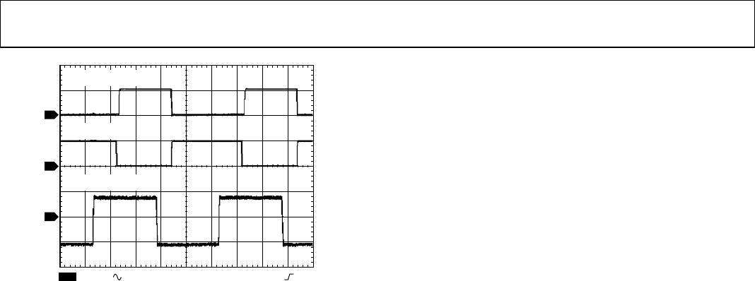
ADDING HYSTERESIS
To prevent oscillations at the output caused by noise or slowly
moving signals passing the switching threshold, each compara-
tor has built-in hysteresis of approximately 9.3 mV. Positive
feedback can be used to increase hysteresis.
For the configuration shown in Figure 31, two resistors are used
to create different switching thresholds, depending on whether
the input signal is increasing or decreasing in magnitude. When
the input voltage is increasing, the threshold is above V
REF
, and
when it is decreasing, the threshold is below V
REF
. V
IN_HI
is the
high input threshold used to trigger the output low to high
transmission. V
IN_LO
is the low input threshold used to trigger
the output high to low transmission.
The upper input threshold level is given by
(
)
R2
R2
R1
+
=
REF
IN_HI
V
V
assuming R
LOAD
>> R2, R
PULLUP
where V
REF
= 0.4 V.
The lower input threshold level is given by
(
)
PULLUP
CC
PULLUP
RR2
R1V
RR2
R1
+
−+
+
=
REF
IN_LO
V
V
The hysteresis is the difference between these voltage levels and
is given by
PULLUP
RR2
R1
+
=∆
CC
IN
V
V
ADCM
P361
06496-031
OUT
OUT
R1
R2
V
IN
V
DD
R
PULLUP
V
REF
= 0.4V
R
LOAD
Figure 31. Comparator Configuration with Added Hysteresis
ADCMP361
V
CC
= 5V
R2 = 1MΩ
R1 = 200kΩ
V
REF
IN+
IN–
V
IN
V
OUT
V
IN
V
IN_LO
V
IN_HI
OUT
06496-132
Figure 32. Noninverting Comparator Configuration with Hysteresis
Rev. B | Page 11 of 12