© 2008 Microchip Technology Inc. DS22116A-page 5
24VL014H
2.0 PIN DESCRIPTIONS
The descriptions of the pins are listed in Table 2-1.
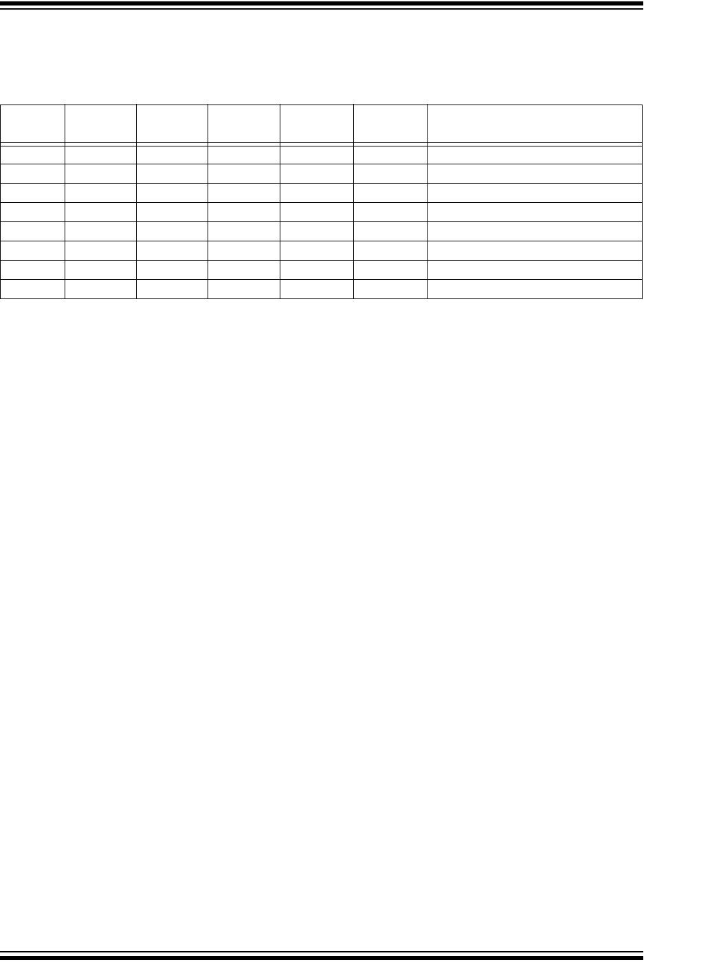
TABLE 2-1: PIN FUNCTION TABLE
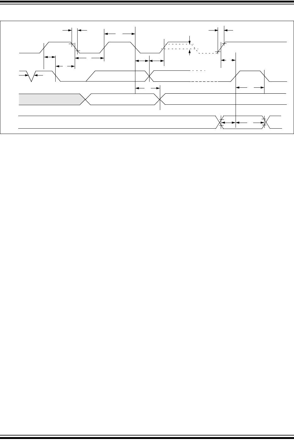
2.1 SDA Serial Data
This is a bidirectional pin used to transfer addresses
and data into and out of the device. It is an open drain
terminal. Therefore, the SDA bus requires a pull-up
resistor to V
CC (typical 10 kΩ for 100 kHz, 2 kΩ for
400 kHz).
For normal data transfer, SDA is allowed to change
only during SCL low. Changes during SCL high are
reserved for indicating the Start and Stop conditions.
2.2 SCL Serial Clock
The SCL input is used to synchronize the data transfer
to and from the device.
2.3 A0, A1, A2
The A0, A1 and A2 inputs are used by the 24VL014H
for multiple device operations. The levels on these
inputs are compared with the corresponding bits in the
slave address. The chip is selected if the compare is
true.
Up to eight 24VL014H devices may be connected to
the same bus by using different Chip Select bit
combinations. These inputs must be connected to
either V
CC or VSS.
In most applications, the chip address inputs A0, A1
and A2 are hard-wired to logic ‘0’ or logic ‘1’. For
applications in which these pins are controlled by a
microcontroller or other programmable device, the chip
address pins must be driven to logic ‘0’ or logic ‘1’
before normal device operation can proceed.
2.4 WP
WP is the hardware write-protect pin. It must be tied to
V
CC or VSS. If tied to VCC, the hardware write protection
is enabled and will protect half of the array (40h-7Fh).
If the WP pin is tied to V
SS the hardware write
protection is disabled.
2.5 Noise Protection
The 24VL014H employs a VCC threshold detector cir-
cuit that disables the internal erase/write logic if the
V
CC is below 1.0 volts at nominal conditions.
The SCL and SDA inputs have Schmitt Trigger and
filter circuits that suppress noise spikes to assure
proper device operation even on a noisy bus.
Name
8-pin
PDIP
8-pin
SOIC
8-pin
TSSOP
8-pin
MSOP
8-pin
TDFN
Function
A0 1 1 1 1 1 User Configurable Chip Select
A1 2 2 2 2 2 User Configurable Chip Select
A2 3 3 3 3 3 User Configurable Chip Select
V
SS 4444 4Ground
SDA 5 5 5 5 5 Serial Data
SCL 6 6 6 6 6 Serial Clock
WP 7 7 7 7 7 Write-Protect Input
V
CC 8 8 8 8 8 +1.5V to 3.6V