LTC1569IS8-6#PBF

1
LTC1569-6
Linear Phase, DC Accurate,
Low Power, 10th Order Lowpass Filter
One External R Sets Cutoff Frequency
Root Raised Cosine Response
3mA Supply Current with a Single 3V Supply
Up to 64kHz Cutoff on a Single 3V Supply
10th Order, Linear Phase Filter in an SO-8
DC Accurate, V
OS(MAX)
= 5mV
Low Power Modes
Differential or Single-Ended Inputs
80dB CMRR (DC)
82dB Signal-to-Noise Ratio, V
S
= 5V
Operates from 3V to ±5V Supplies
The LTC
®
1569-6 is a 10th order lowpass filter featuring
linear phase and a root raised cosine amplitude response.
The high selectivity of the LTC1569-6 combined with its
linear phase in the passband makes it suitable for filtering
both in data communications and data acquisition sys-
Data Communication Filters for 3V Operation
Linear Phase and Phase Matched Filters for I/Q
Signal Processing
Pin Programmable Cutoff Frequency Lowpass Filters
tems.
Furthermore, its root raised cosine response offers
the optimum pulse shaping for PAM data communica-
tions
. The filter attenuation is 50dB at 1.5 • f
CUTOFF
, 60dB
at 2 • f
CUTOFF
, and in excess of 80dB at 6 • f
CUTOFF
. DC-
accuracy-sensitive applications benefit from the 5mV
maximum DC offset.
The LTC1569-6 sampled data filter does not require an
external clock yet its cutoff frequency can be set with a
single external resistor with a typical accuracy of 3.5% or
better
. The external resistor programs an internal oscilla-
tor whose frequency is divided by either 1, 4 or 16 prior to
being applied to the filter network. Pin 5 determines the
divider setting. Thus, up to three cutoff frequencies can be
obtained for each external resistor value. Using various
resistor values and divider settings, the cutoff frequency
can be programmed over a range of six octaves. Alterna-
tively, the cutoff frequency can be set with an external
clock and the clock-to-cutoff frequency ratio is 64:1. The
ratio of the internal sampling rate to the filter cutoff
frequency is 128:1.
The LTC1569-6 is fully tested for a cutoff frequency of
64kHz with a single 3V supply.
The LTC1569-6 features power saving modes and it is
available in an SO-8 surface mount package.
, LTC and LT are registered trademarks of Linear Technology Corporation.
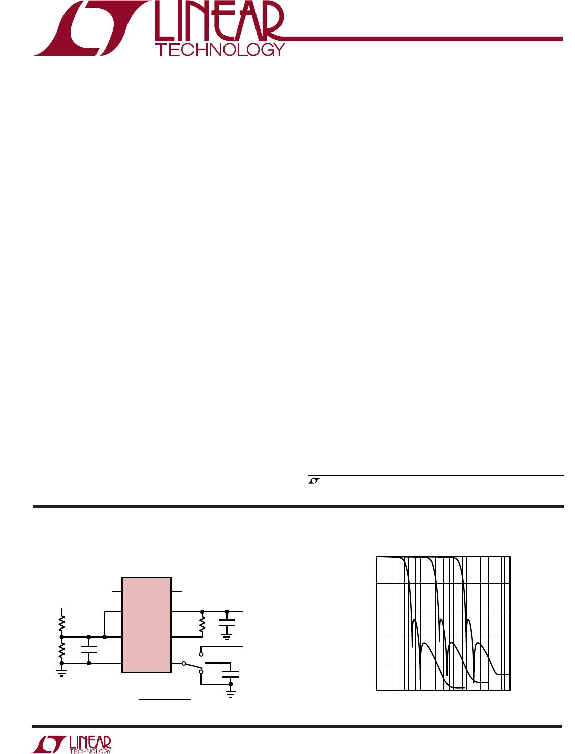
FREQUENCY (kHz)
1
GAIN (dB)
0
–20
–40
–60
–80
100
10 100 1000
1569-6 TA01a
18
27
36
45
1µF
3V
1/4
1/16
1/1
3V
R
EXT
= 10k
100pF
1µF
2k
3.48k
3V
LTC1569-6
EASY TO SET f
CUTOFF
:
f
CUTOFF
=
64kHz (10k/R
EXT
)
1, 4 OR 16
1569-6 TA01
IN
+
IN
GND
V
OUTV
IN
V
OUT
V
+
R
X
DIV/CLK
Frequency Response, f
CUTOFF
= 64kHz/16kHz/4kHz
Single 3V Supply, 64kHz/16kHz/4kHz Lowpass Filter
APPLICATIO S
U
FEATURES
TYPICAL APPLICATIO
U
DESCRIPTIO
U
2
LTC1569-6
A
U
G
W
A
W
U
W
ARB
S
O
LU
T
EXI T
I
S
ORDER PART
NUMBER
WU
U
PACKAGE
/
O
RDER I FOR ATIO
(Note 1)
Total Supply Voltage................................................ 11V
Power Dissipation.............................................. 500mW
Operating Temperature
LTC1569C ............................................... 0°C to 70°C
LTC1569I............................................ 40°C to 85°C
Storage Temperature ............................ 65°C to 150°C
Lead Temperature (Soldering, 10 sec)..................300°C
The denotes the specifications which apply over the full operating temperature range, otherwise specifications are at T
A
= 25°C.
V
S
= 3V (V
+
= 3V, V
= 0V), f
CUTOFF
= 64kHz, R
LOAD
= 10k unless otherwise specified.
E
LECTR
IC
AL C CHARA TERIST
ICS
LTC1569CS8-6
LTC1569IS8-6
S8 PART
MARKING
Consult factory for Military grade parts.
T
JMAX
= 125°C, θ
JA
= 150°C/W
1
2
3
4
8
7
6
5
TOP VIEW
OUT
V
+
R
X
DIV/CLK
IN
+
IN
GND
V
S8 PACKAGE
8-LEAD PLASTIC SO
PARAMETER CONDITIONS MIN TYP MAX UNITS
Filter Gain V
S
= 5V, f
CLK
= 4.096MHz, f
IN
= 1280Hz = 0.02 • f
CUTOFF
–0.05 0.05 0.15 dB
f
CUTOFF
= 64kHz, V
IN
= 1.4V
P-P
,f
IN
= 12.8kHz = 0.2 • f
CUTOFF
0.25 0.15 0.05 dB
R
EXT
= 10k, Pin 5 Shorted f
IN
= 32kHz = 0.5 • f
CUTOFF
0.65 0.55 0.4 dB
to Pin 4 f
IN
= 51.2kHz = 0.8 • f
CUTOFF
1.3 1.0 0.7 dB
f
IN
= 64kHz = f
CUTOFF
5.3 3.8 2.4 dB
f
IN
= 97.5kHz = 1.5 • f
CUTOFF
(LTC1569I) –60 –40 dB
f
IN
= 97.5kHz = 1.5 • f
CUTOFF
(LTC1569C) –60 –48 dB
f
IN
= 128kHz = 2 • f
CUTOFF
–62 –50 dB
f
IN
= 192kHz = 3 • f
CUTOFF
–71 –60 dB
V
S
= 2.7V, f
CLK
= 1MHz, f
IN
= 312Hz = 0.02 • f
CUTOFF
0.12 0.05 0.16 dB
f
CUTOFF
= 15.625kHz, f
IN
= 3125kHz = 0.2 • f
CUTOFF
0.25 0.15 0.05 dB
V
IN
= 1V
P-P
, Pin 6 Shorted f
IN
= 7812kHz = 0.5 • f
CUTOFF
0.65 0.55 0.4 dB
to Pin 4, External Clock f
IN
= 12.5kHz = 0.8 • f
CUTOFF
1.1 0.9 0.7 dB
f
IN
= 15.625kHz = f
CUTOFF
3.6 3.4 3.2 dB
f
IN
= 23.44kHz = 1.5 • f
CUTOFF
(LTC1569I) –54 –48 dB
f
IN
= 23.44kHz = 1.5 • f
CUTOFF
(LTC1569C) –54 –50 dB
f
IN
= 31.25kHz = 2 • f
CUTOFF
(LTC1569I) –60 –52 dB
f
IN
= 31.25kHz = 2 • f
CUTOFF
(LTC1569C) –60 –55 dB
f
IN
= 46.88kHz = 3 • f
CUTOFF
–66 –60 dB
Filter Phase V
S
= 2.7V, f
CLK
= 4MHz, f
IN
= 1250Hz = 0.02 • f
CUTOFF
–11 Deg
f
CUTOFF
= 62.5kHz, Pin 6 f
IN
= 12.5kHz = 0.2 • f
CUTOFF
114 111 –108 Deg
Shorted to Pin 4, f
IN
= 31.25kHz = 0.5 • f
CUTOFF
79 82 85 Deg
External Clock f
IN
= 50kHz = 0.8 • f
CUTOFF
–83 –79 –75 Deg
f
IN
= 62.5kHz = f
CUTOFF
156 162 168 Deg
f
IN
= 93.75kHz = 1.5 • f
CUTOFF
91 Deg
Filter Cutoff Accuracy R
EXT
= 10.24k from Pin 6 to Pin 7, 62.5kHz ±1%
when Self-Clocked V
S
= 3V, Pin 5 Shorted to Pin 4
Filter Output DC Swing V
S
= 3V, Pin 3 = 1.11V 2.1 V
P-P
(Note 6) 1.9 V
P-P
V
S
= 5V, Pin 3 = 2V 3.9 V
P-P
3.7 V
P-P
V
S
= ±5V, Pin 5 Shorted to Pin 7, R
LOAD
= 20k 8.5 V
P-P
15696
1569I6
3
LTC1569-6
The denotes the specifications which apply over the full operating temperature range, otherwise specifications are at T
A
= 25°C.
V
S
= 3V (V
+
= 3V, V
= 0V), f
CLK
= 4.096MHz, f
CUTOFF
= 64kHz, R
LOAD
= 10k unless otherwise specified.
E
LECTR
IC
AL C CHARA TERIST
ICS
PARAMETER CONDITIONS MIN TYP MAX UNITS
Output DC Offset R
EXT
= 10k, Pin 5 Shorted to Pin 7 V
S
= 3V ±2 ±5mV
(Note 2) V
S
= 5V ±6 ±12 mV
V
S
= ±5V ±15 mV
Output DC Offset R
EXT
= 10k, Pin 5 Shorted to Pin 7 V
S
= 3V 25 µV/°C
Drift V
S
= 5V 25 µV/°C
V
S
= ±5V 75 µV/°C
Clock Pin Logic Thresholds V
S
= 3V Min Logical “1” 2.7 V
when Clocked Externally Max Logical “0” 0.5 V
V
S
= 5V Min Logical “1” 4.0 V
Max Logical “0” 0.5 V
V
S
= ±5V Min Logical “1” 4.0 V
Max Logical “0” 0.5 V
Power Supply Current f
CLK
= 256kHz (40k from Pin 6 to Pin 7, V
S
= 3V 3 4 mA
(Note 3) Pin 5 Open, ÷ 4), f
CUTOFF
= 4kHz 5mA
V
S
= 5V 3.5 5 mA
6mA
V
S
= 10V 4.5 7 mA
8mA
f
CLK
= 4.096MHz (10k from Pin 6 to Pin 7, V
S
= 3V 8 mA
Pin 5 Shorted to Pin 4, ÷ 1), f
CUTOFF
= 64kHz 11 mA
V
S
= 5V 9 mA
13 mA
V
S
= 10V 12 mA
17 mA
Clock Feedthrough Pin 5 Open 0.1 mV
RMS
Wideband Noise Noise BW = DC to 2 • f
CUTOFF
95 µV
RMS
THD f
IN
= 3kHz, 1.5V
P-P
, f
CUTOFF
= 32kHz 80 dB
Clock-to-Cutoff 64
Frequency Ratio
Max Clock Frequency V
S
= 3V 5 MHz
(Note 4) V
S
= 5V 5 MHz
V
S
= ±5V 7 MHz
Min Clock Frequency V
S
= 3V, 5V, T
A
< 85°C 1.5 kHz
(Note 5) V
S
= ±5V 3kHz
Input Frequency Range Aliased Components <–65dB 0.9 • f
CLK
Hz
Note 1: Absolute maximum ratings are those values beyond which the life
of a device may be impaired.
Note 2: DC offset is measured with respect to Pin 3.
Note 3: If the internal oscillator is used as the clock source and the divide-
by-4 or divide-by-16 mode is enabled, the supply current is reduced as
much as 40% relative to the divide-by-1 mode.
Note 4: The maximum clock frequency is arbitrarily defined as the
frequency at which the filter AC response exhibits >1dB of gain peaking.
Note 5: The minimum clock frequency is arbitrarily defined as the frequecy
at which the filter DC offset changes by more than 5mV.
Note 6: For more details refer to the Input and Output Voltage Range
paragraph in the Applications Information section.

LTC1569IS8-6#PBF

Mfr. #:
Manufacturer:
Analog Devices Inc.
Description:
Active Filter 10th Order Linear Phase L/Pass Filter
Lifecycle:
New from this manufacturer.
Delivery:
DHL FedEx Ups TNT EMS
Payment:
T/T Paypal Visa MoneyGram Western Union