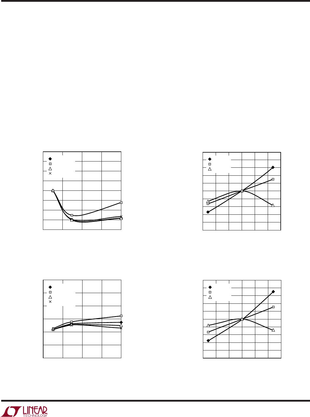
LTC1569IS8-6#PBF

7
LTC1569-6
Using the equation in Figure 1, the approximate filter
cutoff frequency is f
CUTOFF
= 64kHz • (10k/20k)
• (1/16) = 2kHz.
For a more precise f
CUTOFF
estimate, use Table 1 to get
a value of f
CUTOFF
when R
EXT
= 20k and use the graph
in Figure 6 to find the correct divide ratio when V
S
= 3V
and R
EXT
= 20k. Based on Table 1 and Figure 6, f
CUTOFF
= 32kHz • (20.18k/20k) • (1/16.02) = 2.01kHz.
From Table 1, the part-to-part variation of f
CUTOFF
will
be ±2%. From the graph in Figure 7, the 0°C to 70°C
drift of f
CUTOFF
will be –0.2% to 0.2%.
Example 2: LTC1569-6, R
EXT
= 10k, V
S
= 5V, divide-by-1
mode, DIV/CLK (Pin␣ 5) connected to V
(Pin 4), T
A
= 25°C.
APPLICATIONS INFORMATION
WUU
U
Using the equation in Figure 1, the approximate filter
cutoff frequency is f
CUTOFF
= 64kHz • (10k/10k)
• (1/1) = 64kHz.
For a more precise f
CUTOFF
estimate, use Figure 2 to
correct for the supply voltage when V
S
= 5V. From
Table␣ 1 and Figure 2, f
CUTOFF
= 64k • (10k/10k) • 0.970
= 62.1kHz.
The oscillator is sensitive to transients on the positive
supply. The IC should be soldered to the PC board and the
PCB layout should include a 1µF ceramic capacitor be-
tween V
+
(Pin 7) and V
(Pin 4) , as close as possible to
the IC to minimize inductance. Avoid parasitic capacitance
on R
X
and avoid routing noisy signals near R
X
(Pin 6). Use
Figure 4. Typical Divide Ratio in the
Divide-by-4 Mode, T
A
= 25°C
Figure 5. Filter Cutoff vs Temperature,
Divide-by-4 Mode, R
EXT
= 10k
Figure 3. Filter Cutoff vs Temperature,
Divide-by-1 Mode, R
EXT
= 10k
Figure 2. Filter Cutoff vs V
SUPPLY
,
Divide-by-1 Mode, T
A
= 25°C
V
SUPPLY
(V)
2
DIVIDE RATIO
1569-6 F04
4.08
4.04
4.00
3.96
4 6 810
R
EXT
= 5k
R
EXT
= 10k
R
EXT
= 20k
R
EXT
= 40k
TEMPERATURE (°C)
–50
NORMALIZED FILTER CUTOFF
1569-6 F05
1.010
1.008
1.006
1.004
1.002
1.000
0.998
0.996
0.994
0.992
0.990
–25
0 25 50 75 100
V
S
= 3V
V
S
= 5V
V
S
= 10V
V
SUPPLY
(V)
2
NORMALIZED FILTER CUTOFF
1569-6 F02
1.04
1.03
1.02
1.01
1.00
0.99
0.98
0.97
0.96
4 6 810
R
EXT
= 5k
R
EXT
= 10k
R
EXT
= 20k
R
EXT
= 40k
TEMPERATURE (°C)
–50
NORMALIZED FILTER CUTOFF
1569-6 F03
1.010
1.008
1.006
1.004
1.002
1.000
0.998
0.996
0.994
0.992
0.990
–25
0 25 50 75 100
V
S
= 3V
V
S
= 5V
V
S
= 10V
8
LTC1569-6
APPLICATIONS INFORMATION
WUU
U
Figure 6. Typical Divide Ratio in the
Divide-by-16 Mode, T
A
= 25°C
Figure 7. Filter Cutoff vs Temperature,
Divide-by-16 Mode, R
EXT
= 10k
TEMPERATURE (°C)
–50
NORMALIZED FILTER CUTOFF
1569-6 F07
1.010
1.008
1.006
1.004
1.002
1.000
0.998
0.996
0.994
0.992
0.990
–25
0 25 50 75 100
V
S
= 3V
V
S
= 5V
V
S
= 10V
V
SUPPLY
(V)
2
DIVIDE RATIO
1569-6 F06
16.32
16.16
16.00
15.84
4 6 810
R
EXT
= 5k
R
EXT
= 10k
R
EXT
= 20k
R
EXT
= 40k
a ground plane connected to V
(Pin 4) for single supply
applications. Connect a ground plane to GND (Pin 3) for
dual supply applications and connect V
(Pin 4) to a
copper trace with low thermal resistance.
Input and Output Voltage Range
The input signal range includes the full power supply
range. The output range is typically (V
+ 50mV) to (V
+
0.8V) when using a single 3V supply with the GND (Pin 3)
voltage set to 1.11V. In other words, the output range is
typically 2.1V
P-P
for a 3V supply. Similarly, the output
range is typically 3.9V
P-P
for a single 5V supply when the
GND (Pin 3) voltage is 2V. For ±5V supplies, the output
range is typically 8.5V
P-P
.
The LTC1569-6 can be driven with a single-ended or
differential signal. When driven differentially, the voltage
between IN
+
and IN
(Pin 1 and Pin 2) is filtered with a DC
gain of 1. The single-ended output voltage OUT (Pin 8) is
referenced to the voltage of the GND (Pin 3). The common
mode voltage of IN
+
and IN
can be any voltage that keeps
the input signals within the power supply range.
For noninverting single-ended applications, connect IN
to GND or to a quiet DC reference voltage and apply the
input signal to IN
+
. If the input is DC coupled then the DC
gain from IN
+
to OUT will be 1. This is true given IN
+
and
OUT are referenced to the same voltage, i.e., GND, V
or
some other DC reference. To achieve the distortion levels
shown in the Typical Performance Characteristics the
input signal at IN
+
should be centered around the DC
voltage at IN
. The input can also be AC coupled, as shown
in the Typical Applications section.
For inverting single-ended filtering, connect IN
+
to GND or
to quiet DC reference voltage. Apply the signal to IN
. The
DC gain from IN
to OUT is –1, assuming IN
is referenced
to IN
+
and OUT is reference to GND.
Refer to the Typical Performance Characteristics section
to estimate the THD for a given input level.
Dynamic Input Impedance
The unique input sampling structure of the LTC1569-6 has
a dynamic input impedance which depends on the con-
figuration, i.e., differential or single-ended, and the clock
frequency. The equivalent circuit in Figure 8 illustrates the
input impedance when the cutoff frequency is 64kHz. For
other cutoff frequencies replace the 125k value with
125k • (64kHz/f
CUTOFF
).
When driven with a single-ended signal into IN
with IN
+
tied to GND, the input impedance is very high (~10M).
When driven with a single-ended signal into IN
+
with IN
tied to GND, the input impedance is a 125k resistor to GND.
When driven with a complementary signal whose com-
mon mode voltage is GND, the IN
+
input appears to have
125k to GND and the IN
input appears to have –125k to
GND. To make the effective IN
impedance 125k when
driven differentially, place a 62.5k resistor from IN
to
GND. For other cutoff frequencies use 62.5k • (64kHz/
9
LTC1569-6
DC Accuracy
DC accuracy is defined as the error in the output voltage
after DC offset and DC gain errors are removed. This is
similar to the definition of the integral nonlinearity in A/D
converters. For example, after measuring values of V
OUT(DC)
vs V
IN(DC)
for a typical LTC1569-6, a linear regression
shows that V
OUT(DC)
= V
IN(DC)
• 0.99854 + 0.00134V is the
straight line that best fits the data. The DC accuracy
describes how much the actual data deviates from this
straight line (i.e., DCERROR = V
OUT(DC)
– (V
IN(DC)
• 0.99854
+ 0.00134V). In a 12-bit system with a full-scale value of
2V, the LSB is 488µV. Therefore, if the DCERROR of the
filter is less than 488µV over a 2V range, the filter has
12-bit DC accuracy. Figure 9 illustrates the typical DC
accuracy of the LTC1569-6 on a single 5V supply.
DC Offset
The output DC offset of the LTC1569-6 is trimmed to less
than ±5mV. The trimming is performed with V
S
= 1.9V,
–1.1V with the filter cutoff frequency set to 4kHz (R
EXT
=
10k, DIV/CLK shorted to V
+
). To obtain optimum DC offset
performance, appropriate PC layout techniques should be
used. The filter IC should be soldered to the PC board. The
power supplies should be well decoupled including a 1µF
ceramic capacitor from V
+
(Pin 7) to V
(Pin 4). A ground
plane should be used. Noisy signals should be isolated
from the filter input pins.
When the power supply is 3V, the output DC offset should
change less than ±2mV when the clock frequency varies
from 64kHz to 4096kHz. When the clock frequency is
fixed, the output DC offset will typically change by less
than ±3mV (±15mV) when the power supply varies from
3V to 5V (±5V) in the divide-by-1 mode. In the divide-by-
4 or divide-by-16 modes, the output DC offset will typically
change less than –9mV (–27mV) when the power supply
varies from 3V to 5V (±5V). The offset is measured with
respect to GND (Pin 3).
Aliasing
Aliasing is an inherent phenomenon of sampled data
filters. In lowpass filters significant aliasing only occurs
when the frequency of the input signal approaches the
sampling frequency or multiples of the sampling fre-
APPLICATIONS INFORMATION
WUU
U
f
CUTOFF
), as shown in the Typical Applications section. The
typical variation in dynamic input impedance for a given
clock frequency is ±10%.
Wideband Noise
The wideband noise of the filter is the RMS value of the
device’s output noise spectral density. The wideband
noise data is used to determine the operating signal-to-
noise at a given distortion level. The wideband noise is
nearly independent of the value of the clock frequency and
excludes the clock feedthrough. Most of the wideband
noise is concentrated in the filter passband and cannot be
removed with post filtering (Table 2). Table 3 lists the
typical wideband noise for each supply.
Table 2. Wideband Noise vs Supply Voltage, Single 3V Supply
Bandwidth Total Integrated Noise
DC to f
CUTOFF
80µV
RMS
DC to 2 • f
CUTOFF
95µV
RMS
DC to f
CLK
110µV
RMS
Table 3. Wideband Noise vs Supply Voltage, f
CUTOFF
= 64kHz
Total Integrated Noise
Power Supply DC to 2 • f
CUTOFF
3V 95µV
RMS
5V 100µV
RMS
±5V 105µV
RMS
Clock Feedthrough
Clock feedthrough is defined as the RMS value of the clock
frequency and its harmonics that are present at the filter’s
OUT pin (Pin 8). The clock feedthrough is measured with
IN
+
and IN
(Pins 1 and 2) grounded and depends on the
PC board layout and the power supply decoupling. Table␣ 4
shows the clock feedthrough (the RMS sum of the first 11
harmonics) when the LTC1569-6 is self-clocked with
R
EXT
= 10k, DIV/CLK (Pin 5) open (divide-by-4 mode). The
clock feedthrough can be reduced with a simple RC post
filter.
Table 4. Clock Feedthrough
Power Supply Feedthrough
3V 0.1mV
RMS
5V 0.3mV
RMS
±5V 0.9mV
RMS

LTC1569IS8-6#PBF

Mfr. #:
Manufacturer:
Analog Devices Inc.
Description:
Active Filter 10th Order Linear Phase L/Pass Filter
Lifecycle:
New from this manufacturer.
Delivery:
DHL FedEx Ups TNT EMS
Payment:
T/T Paypal Visa MoneyGram Western Union