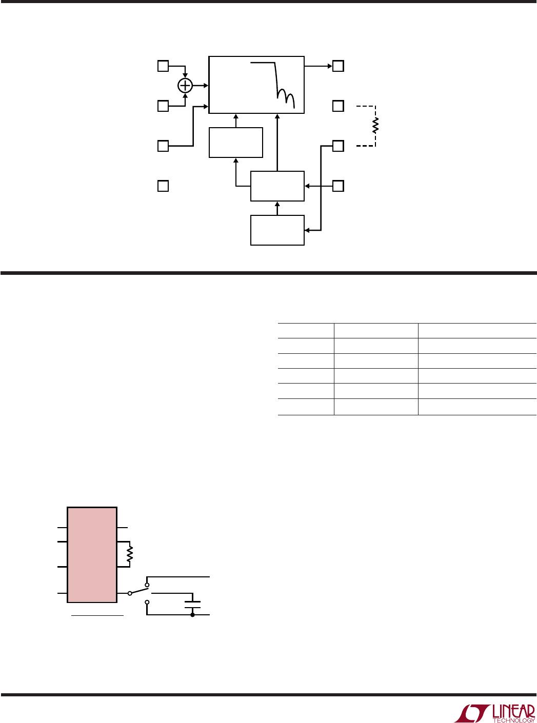
LTC1569IS8-6#PBF

4
LTC1569-6
TYPICAL PERFOR A CE CHARACTERISTICS
UW
THD vs Input VoltageTHD vs Input Frequency
INPUT VOLTAGE (V
P-P
)
0
0.5 1.0 1.5 2.0 2.5 3.0 3.5 4.0
THD (dB)
1569-6 G04
–50
–55
–60
–65
–70
–75
–80
–85
–90
f
IN
= 3kHz
f
CUTOFF
= 32kHz
IN
+
TO OUT
V
S
= 5V
PIN 3 = 2V
V
S
= 3V
PIN 3 = 1.11V
INPUT FREQUENCY (kHz)
0
5 10 15 20 25 30
THD (dB)
1569-6 G03
–60
–65
–70
–75
–80
–85
–90
V
IN
= 1.5V
P-P
f
CUTOFF
= 32kHz
IN
+
TO OUT
V
S
= 5V
PIN 3 = 2V
FREQUENCY (kHz)
GAIN (dB)
10
–10
–30
–50
–70
–90
102.5 100 1000
1569-6 G01
FREQUENCY (kHz)
GAIN (dB)
1
0
–1
–2
–3
–4
DELAY (µs)
40
36
32
28
24
20
10.2 10 80
1569-6 GO2
f
CUTOFF
(kHz)
0.1
I
SUPPY
(mA)
11
10
9
8
7
6
5
4
3
1 10 100
1569-6 G06
DIV-BY-1
DIV-BY-4
EXT CLK
DIV-BY-16
f
CUTOFF
(kHz)
0.1
I
SUPPY
(mA)
14
12
10
8
6
4
1 10 100
1569-6 G07
DIV-BY-1
DIV-BY-4
EXT CLK
DIV-BY-16
3V Supply Current
Passband Gain and Group Delay
vs Frequency
Gain vs Frequency
f
CUTOFF
(kHz)
0.1
I
SUPPY
(mA)
10
9
8
7
6
5
4
3
2
1 10 100
1569-6 G05
DIV-BY-1
DIV-BY-4
EXT CLK
DIV-BY-16
5V Supply Current ±5V Supply Current
5
LTC1569-6
PIN FUNCTIONS
UUU
IN
+
/IN
(Pins 1, 2): Signals can be applied to either or
both input pins. The DC gain from IN
+
(Pin 1) to OUT
(Pin␣ 8) is 1.0, and the DC gain from Pin 2 to Pin 8 is –1. The
input range, input resistance and output range are de-
scribed in the Applications Information section. Input
voltages which exceed the power supply voltages should
be avoided. Transients will not cause latchup if the current
into/out of the input pins is limited to 20mA.
GND (Pin 3): The GND pin is the reference voltage for the
filter and should be externally biased to 2V (1.11V) to
maximize the dynamic range of the filter in applications
using a single 5V (3V) supply. For single supply operation,
the GND pin should be bypassed with a quality 1µF
ceramic capacitor to V
(Pin 4). The impedance of the
circuit biasing the GND pin should be less than 2k as the
GND pin generates a small amount of AC and DC current.
For dual supply operation, connect Pin␣ 3 to a high quality
DC ground. A ground plane should be used. A poor ground
will increase DC offset, clock feedthrough, noise and
distortion.
V
/V
+
(Pins 4, 7): For 3V, 5V and ±5V applications a
quality 1µF ceramic bypass capacitor is required from V
+
(Pin 7) to V
(Pin 4) to provide the transient energy for the
internal clock drivers. The bypass should be as close as
possible to the IC. In dual supply applications (Pin 3 is
grounded), an additional 0.1µF bypass from V
+
(Pin 7) to
GND (Pin 3) and V
(Pin 4) to GND (Pin 3) is recom-
mended.
The maximum voltage difference between GND (Pin 3) and
V
+
(Pin 7) should not exceed 5.5V.
DIV/CLK (Pin 5): DIV/CLK serves two functions. When the
internal oscillator is enabled, DIV/CLK can be used to
engage an internal divider. The internal divider is set to 1:1
when DIV/CLK is shorted to V
(Pin 4). The internal divider
is set to 4:1 when DIV/CLK is allowed to float (a 100pF
bypass to V
is recommended). The internal divider is set
to 16:1 when DIV/CLK is shorted to V
+
(Pin 7). In the
divide-by-4 and divide-by-16 modes the power supply
current is reduced by as much as 40%.
When the internal oscillator is disabled (R
X
shorted
to V
) DIV/CLK becomes an input pin for applying an
external clock signal. For proper filter operation, the clock
waveform should be a squarewave with a duty cycle as
close as possible to 50% and CMOS voltages levels (see
Electrical Characteristics section for voltage levels). DIV/
CLK pin voltages which exceed the power supply voltages
should be avoided. Transients will not cause latchup if the
fault current into/out of the DIV/CLK pin is limited to 40mA.
R
X
(Pin 6): Connecting an external resistor between the R
X
pin and V
+
(Pin 7) enables the internal oscillator. The value
of the resistor determines the frequency of oscillation. The
maximum recommended resistor value is 40k and the
minimum is 3.8k. The internal oscillator is disabled by
shorting the R
X
pin to V
(Pin 4). (Please refer to the
Applications Information section.)
OUT (Pin 8): Filter Output. This pin can drive 10k and/or
40pF loads. For larger capacitive loads, an external 100
series resistor is recommended. The output pin can ex-
ceed the power supply voltages by up to ±2V without
latchup.
6
LTC1569-6
BLOCK DIAGRA
W
10TH ORDER
LINEAR PHASE
FILTER NETWORK
POWER
CONTROL
DIVIDER/
BUFFER
R
EXT
PRECISION
OSCILLATOR
5
6
7
8
4
3
2
1 OUT
V
+
R
X
DIV/CLK
IN
+
IN
GND
V
1569-6 BD
APPLICATIONS INFORMATION
WUU
U
Self-Clocking Operation
The LTC1569-6 features a unique internal oscillator which
sets the filter cutoff frequency using a single external
resistor
. The design is optimized for V
S
= 3V, f
CUTOFF
=
64kHz, where the filter cutoff frequency error is typically
<1% when a 0.1% external 10k resistor is used. With
different resistor values and internal divider settings, the
cutoff frequency can be accurately varied from 1kHz to
64kHz. As shown in Figure 1, the divider is controlled by
the DIV/CLK (Pin 5). Table 1 summarizes the cutoff
frequency vs external resistor values for the divide-by-1
mode.
LTC1569-6
18
27
36
45
DIVIDE-BY-4
DIVIDE-BY-1
DIVIDE-BY-16
V
+
V
R
EXT
100pF
f
CUTOFF
=
64kHz (10k/R
EXT
)
1, 4 OR 16
1569-6 F01
IN
+
IN
GND
V
OUT
V
+
R
X
DIV/CLK
Figure 1
Table1. f
CUTOFF
vs R
EXT
, V
S
= 3V, T
A
= 25°C, Divide-by-1 Mode
R
EXT
Typical f
CUTOFF
Typical Variation of f
CUTOFF
3844* N/A ±3.0%
5010* N/A ±2.5%
10k 64kHz ±1%
20.18k 32kHz ±2.0%
40.2k 16kHz ±3.5%
*R
EXT
values less than 10k can be used only in the divide-by-16 mode.
In the divide-by-4 and divide-by-16 modes, the cutoff
frequencies in Table 1 will be lowered by 4 and 16
respectively. When the LTC1569-6 is in the divide-by-4
and divide-by-16 modes the power is automatically re-
duced. This results in up to a 40% power savings.
The power reduction in the divide-by-4 and divide-by-16
modes, however, effects the fundamental oscillator fre-
quency. Hence, the effective divide ratio will be slightly
different from 4:1 or 16:1 depending on V
S
, T
A
and R
EXT
.
Typically this error is less than 1% (Figures 4 and 6).
The cutoff frequency is easily estimated from the equation
in Figure 1. Examples 1 and 2 illustrate how to use the
graphs in Figures 2 through 7 to get a more precise
estimate of the cutoff frequency.
Example 1: LTC1569-6, R
EXT
= 20k, V
S
= 3V, divide-by-16
mode, DIV/CLK (Pin␣ 5) connected to V
+
(Pin 7), T
A
= 25°C.

LTC1569IS8-6#PBF

Mfr. #:
Manufacturer:
Analog Devices Inc.
Description:
Active Filter 10th Order Linear Phase L/Pass Filter
Lifecycle:
New from this manufacturer.
Delivery:
DHL FedEx Ups TNT EMS
Payment:
T/T Paypal Visa MoneyGram Western Union