REV. A
AD7709
–12–
As shown in the block diagram, the Sinc
3
filter outputs alternately
contain +V
OS
and –V
OS
, where V
OS
is the respective channel offset.
This offset is removed by performing a running average of 2, which
means that the settling time to any change in programming of
the ADC will be twice the normal conversion time, while an
asynchronous step change on the analog input will not be fully
reflected until the third subsequent output.
t
f
t
SETTLE
ADC
ADC
=
Ê
Ë
Á
ˆ
¯
˜
2
2
The allowable range for SF is 13 to 255, with a default of 69
(45H). The corresponding conversion rates, conversion times,
and settling times are shown in Table I. Note that the conver-
sion time increases by 0.732 ms for each increment in SF.
FREQUENCY – Hz
0
–140
–200
0
650
50
100
150 200 250 300 350 400
450 500 550 600
700
ATTENUATION – dB
–20
–120
–160
–180
–60
–100
–40
–80
SF = 13
OUTPUT DATA RATE = 105Hz
INPUT BANDWIDTH = 25.2Hz
FIRST NOTCH = 52.5Hz
50Hz REJECTION = –23.6dB, 50Hz 1Hz REJECTION = –20.5dB
60Hz REJECTION = –14.6dB, 60Hz 1Hz REJECTION = –13.6dB
Figure 5. Filter Profile with SF = 13
FREQUENCY – Hz
0
–80
–160
0 10010
ATTENUATION – dB
20 30 40 50 60 70 80 90
–20
–40
–120
–140
–60
–100
SF = 82
OUTPUT DATA RATE = 16.65Hz
INPUT BANDWIDTH = 4Hz
50Hz REJECTION = –171dB, 50Hz 1Hz REJECTION = –100dB
60Hz REJECTION = –58dB, 60Hz 1Hz REJECTION = –53dB
Figure 6. Filter Profile with SF = 82
Table I. ADC Conversion and Settling Times for Various
SF Words
Data Update Rate Settling Time
SF Word f
ADC
(Hz) t
SETTLE
(ms)
13 105.3 19.04
69 (Default) 19.79 101.07
255 5.35 373.54
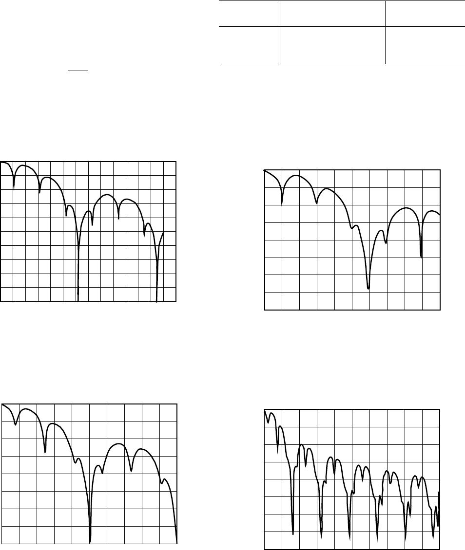
Normal mode rejection is the major function of the digital filter
on the AD7709. The normal mode 50 ± 1 Hz rejection with an
SF word of 82 is typically –100 dB. The 60 ± 1 Hz rejection with
SF = 68 is typically –100 dB. Simultaneous 50 Hz and 60 Hz
rejection of better than 60 dB is achieved with an SF of 69.
Choosing an SF word of 69 places notches at both 50 Hz and
60 Hz. Figures 5 to 8 show the filter rejection for a selection
of SF words.
FREQUENCY – Hz
0
–80
–160
0 100
10
ATTENUATION – dB
20 30 40 50 60 70 80 90
–20
–40
–120
–140
–60
–100
SF = 69
OUTPUT DATA RATE = 19.8Hz
INPUT BANDWIDTH = 4.74Hz
FIRST NOTCH = 9.9Hz
50Hz REJECTION = –66dB, 50Hz 1Hz REJECTION = –60dB
60Hz REJECTION = –117dB, 60Hz 1Hz REJECTION = –94dB
Figure 7. Filter Profile with Default SF = 69 Giving Filter
Notches at Both 50 Hz and 60 Hz
FREQUENCY – Hz
0
–80
–160
0 10010
ATTENUATION – dB
20 30 40 50 60 70 80 90
–20
–40
–120
–140
–60
–100
SF = 255
OUTPUT DATA RATE = 5.35Hz
INPUT BANDWIDTH = 1.28Hz
50Hz REJECTION = –93dB, 50Hz 1Hz REJECTION = –93dB
60Hz REJECTION = –74dB, 60Hz 1Hz REJECTION = –68dB
Figure 8. Filter Profile with SF = 255
REV. A
AD7709
–13–
NOISE PERFORMANCE
Tables II and III show the output rms noise and output peak-to-
peak resolution in bits (rounded to the nearest 0.5 LSB) for a
selection of output update rates. The numbers are typical and
generated at a differential input voltage of 0 V. The output update
rate is selected via the SF7–SF0 bits in the Filter Register. It is
important to note that the peak-to-peak resolution figures
represent the resolution for which there will be no code flicker
within a six-sigma limit. The output noise comes from two sources.
The first is the electrical noise in the semiconductor devices
(device noise) used in the implementation of the modulator.
Second, when the analog input is converted into the digital
domain, quantization noise is added. The device noise is at a low
DIN
ADC STATUS REGISTER
(8 BITS)
CONFIGURATION REGISTER
(24 BITS)
FILTER REGISTER
(8 BITS)
ADC DATA REGISTER
(16 BITS)
REGISTER
SELECT
DECODER
DOUT
DOUT
DOUT
DOUT
DOUT
DIN
DIN
WEN
R/W STBY
OSCPD 0 0 A1 A0
Figure 9. On-Chip Registers
level and is independent of frequency. The quantization noise starts
at an even lower level but rises rapidly with increasing frequency
to become the dominant noise source.
The numbers in the tables
are given for the bipolar input ranges.
For the unipolar ranges,
the rms noise numbers will be the same
as the bipolar range, but
the peak-to-peak resolution is now based
on half the signal range,
which effectively means losing 1 bit of resolution.
ON-CHIP REGISTERS
The AD7709 is controlled and configured via a number of on-chip
registers, as shown in Figure 9 and described in more detail in the
following pages. In the following descriptions, set implies a Logic 1
state and cleared implies a Logic 0 state, unless otherwise stated.
Table II. Typical Output RMS Noise vs. Input Range and Update Rate for the AD7709 (Output RMS Noise in V)
SF Data Update
Input Range
Word Rate (Hz) 20 mV 40 mV 80 mV 160 mV 320 mV 640 mV 1.28 V 2.56 V
13 105.3 1.50 1.50 1.60 1.75 3.50 4.50 6.70 11.75
69 19.79 0.60 0.65 0.65 0.65 0.65 0.95 1.40 2.30
255 5.35 0.35 0.35 0.37 0.37 0.37 0.51 0.82 1.25
Table III. Peak-to-Peak Resolution vs. Input Range and Update Rate for the AD7709 (Peak-to-Peak Resolution in Bits)
SF Data Update
Input Range
Word Rate (Hz) 20 mV 40 mV 80 mV 160 mV 320 mV 640 mV 1.28 V 2.56 V
13 105.3 12 13 14 15 15 15.5 16 16
69 19.79 13 14 15 16 16 16 16 16
255 5.35 14 15 16 16 16 16 16 16
REV. A
AD7709
–14–
Communications Register (A1, A0 = 0, 0)
The Communications Register is an 8-bit write-only register. All communications to the part must start with a write operation to the
Communications Register. The data written to the Communications Register determines whether the next operation is a read or
write operation, and to which register this operation takes place. For read or write operations, once the subsequent read or write
operation to the selected register is complete, the interface returns to where it expects a write operation to the Communications
Register. This is the default state of the interface, and on power-up or after a RESET, the AD7709 is in this default state waiting for
a write operation to the Communications Register. In situations where the interface sequence is lost, a write operation of at least 32
serial clock cycles with DIN high, returns the AD7709 to this default state by resetting the part. Table IV outlines the bit designations for
the Communications Register. CR0 to CR7 indicate the bit location, CR denoting the bits are in the Communications Register.
CR7
denotes the first bit of the data stream.
7RC6RC5RC4RC3RC2RC1RC0RC
NEW )0(
/R W )0()0(YBTS)0(DPCSO)0(0)0(0)0(1A)0(A
Table IV. Communications Register Bit Designations
Bit Bit
Location Name Description
CR7 WEN Write Enable Bit.
A 0 must be written to this bit so the write operation to the Communications Register
actually takes place.
If a 1 is written to this bit, the part will not clock on to subsequent bits in the register.
It will stay at this
bit location until a 0 is written to this bit. Once a 0 is written to the WEN bit, the next seven bits will be
loaded to the Communications Register.
CR6 R/W A 0 in this bit location indicates that the next operation will be a write to a specified register.
A 1 in this position indicates that the next operation will be a read from the designated register.
CR5 STBY Standby Bit Location.
A 1 in this location places the AD7709 in low power mode.
A 0 in this location powers up the AD7709.
CR4 OSCPD Oscillator Power-Down Bit.
If this bit is set, placing the AD7709 in standby mode will stop the crystal oscillator also, reducing the
power consumed by the part to a minimum. The oscillator will require 300 ms to begin oscillating when
the ADC is taken out of power-down mode.
If this bit is cleared, the oscillator is not stopped when the ADC is placed in power-down mode. When
the ADC is taken out of power-down mode, the oscillator does not require the 300 ms start-up time.
CR3–CR2 0 These bits must be programmed with a Logic 0 for correct operation.
CR1–CR0 A1–A0 Register Address Bits. These address bits are used to select which of the AD7709 registers are accessed
during this serial interface communication.
Table V. Register Selection Table
A1 A0 Register
00Communications Register during a Write Operation
00Status Register during a Read Operation
01Configuration Register
10Filter Register
11ADC Data Register
AD7709BRUZ

Mfr. #:
Manufacturer:
Analog Devices Inc.
Description:
Analog to Digital Converters - ADC 16-Bit w/ Current Sources
Lifecycle:
New from this manufacturer.
Delivery:
DHL FedEx Ups TNT EMS
Payment:
T/T Paypal Visa MoneyGram Western Union