REV. A
AD7709
–21–
AD7709-to-68HC11 Interface
Figure 11 shows an interface between the AD7709 and the
68HC11 microcontroller. The diagram shows the minimum
(3-wire) interface with CS on the AD7709 hardwired low. In this
scheme, the RDY bit of the Status Register is monitored to
determine when the Data Register is updated. An alternative
scheme, which increases the number of interface lines to four, is to
monitor the RDY output line from the AD7709. The monitoring
of the RDY line can be done in two ways. First, RDY can be
connected to one of the 68HC11 port bits (such as PC0), which
is configured as an input. This port bit is then polled to determine
the status of RDY. The second scheme is to use an interrupt
driven system, in which case the RDY output is connected to
the IRQ input of the 68HC11. For interfaces that require
control of the CS input on the AD7709, one of the port bits of the
68HC11 (such as PC1), which is configured as an output, can
be used to drive the CS input.
The 68HC11 is configured in the master mode with its CPOL
bit set to a Logic 1 and its CPHA bit set to a Logic 1. When the
68HC11 is configured like this, its SCLK line idles high between
data transfers. The AD7709 is not capable of full-duplex opera-
tion. If the AD7709 is configured for a write operation, no data
appears on the DOUT lines even when the SCLK input is active.
Similarly, if the AD7709 is configured for a read operation, data
presented to the part on the DIN line is ignored even when
SCLK is active.
68HC11
V
DD
AD7709
SS
SCK
MISO
MOSI
RESET
DOUT
DIN
CS
SCLK
V
DD
Figure 11. AD7709-to-68HC11 Interface
AD7709-to-8051 Interface
An interface circuit between the AD7709 and the 8XC51 microcon-
troller is shown in Figure 12. The diagram shows the minimum
number of interface connections with CS on the AD7709 hard-
wired low. In the case of the 8XC51 interface, the minimum
number of interconnects is just two. In this scheme, the RDY
bit of the Status Register is monitored to determine when the
Data Register is updated. The alternative scheme, which increases
the number of interface lines to three, is to monitor the RDY output
line from the AD7709. The monitoring of the RDY line can be
done in two ways. First, RDY can be connected to one of the
8XC51 port bits (such as P1.0) which is configured as an input.
This port bit is then polled to determine the status of RDY.
8XC51
V
DD
AD7709
P3.0
P3.1
RESET
DIN
SCLK
CS
DOUT
V
DD
10k
Figure 12. AD7709-to-8XC51 Interface
The second scheme is to use an interrupt-driven system, in which
case the RDY output is connected to the INT1 input of the
8XC51. For interfaces that require control of the CS input on
the AD7709, one of the port bits of the 8XC51 (such as P1.1),
which is configured as an output, can be used to drive the CS
input. The 8XC51 is configured in its Mode 0 serial interface
mode. Its serial interface contains a single data line. As a result,
the DOUT and DIN pins of the AD7709 should be connected
together with a 10 kW pull-up resistor. The serial clock on the
8XC51 idles high between data transfers. The 8XC51 outputs
the LSB first in a write operation, while the AD7709 expects the
MSB first so the data to be transmitted has to be rearranged
before being written to the output serial register. Similarly, the
AD7709 outputs the MSB first during a read operation while
the 8XC51 expects the LSB first. Therefore, the data read into
the serial buffer needs to be rearranged before the correct data
word from the AD7709 is available in the accumulator.
ADSP-2103/
ADSP-2105
V
DD
AD7709
RFS
SCLK
RESET
DOUT
DIN
SCLK
CS
TFS
DR
DT
Figure 13. AD7709-to-ADSP-2103/ADSP-2105 Interface
AD7709-to-ADSP-2103/ADSP-2105 Interface
Figure 13 shows an interface between the AD7709 and the
ADSP-2103/ADSP-2105 DSP processor. In the interface shown,
the RDY bit of the Status Register is again monitored to
determine when the Data Register is updated. The alternative
scheme is to use an interrupt-driven system, in which case the
REV. A
AD7709
–22–
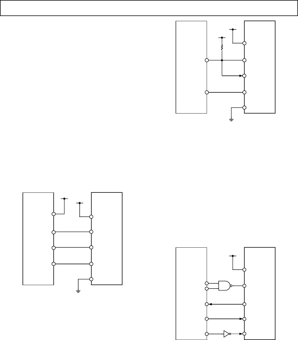
RDY output is connected to the IRQ2 input of the ADSP-2103/
ADSP-2105. The serial interface of the ADSP-2103/ADSP-2105
is set up for alternate framing mode. The RFS and TFS pins of
the ADSP-2103/ADSP-2105 are configured as active low
outputs and the ADSP-2103/ADSP-2105 serial clock line, SCLK,
is also configured as an output. The CS for the AD7709 is
active when either the RFS or TFS outputs from the ADSP-2103/
ADSP-2105 are active. The serial clock rate on the ADSP-2103/
ADSP-2105 should be limited to 3 MHz to ensure correct opera-
tion with the AD7709.
CIRCUIT DESCRIPTION
The AD7709 is a - A/D converter with on-chip digital filtering,
intended for the measurement of wide dynamic range, low
frequency signals such as those in weigh scale, pressure, tempera-
ture, industrial control, or process control applications. It employs
a - conversion technique to realize up to 16 bits of no-missing-
codes performance. The - modulator converts the sampled
input signal into a digital pulse train whose duty cycle contains
the digital information. A Sinc
3
programmable low-pass filter is
then employed to decimate the modulator output data stream to
give a valid data conversion result at programmable output rates
from 5.35 Hz (186.77 ms) to 105.03 Hz (9.52 ms). A chopping
scheme is also employed to minimize ADC offset and offset and
gain drift errors. The channel is buffered and can be programmed
for one of eight input ranges from ± 20 mV to ± 2.56 V. The input
channels can be configured for either fully differential inputs or
pseudo-differential input channels via the CH2, CH1, and CH0
bits in the Configuration Register. Buffering the input channel
allows the part to handle significant source impedances on the
analog input, allowing R/C filtering (for noise rejection or RFI
reduction) to be placed on the analog inputs if required. These
input channels are intended for converting signals directly from
sensors without the need for external signal conditioning. Other
functions contained on-chip that augment the operation of the
ADC include software configurable current sources, switchable
reference inputs, and low-side power switches.
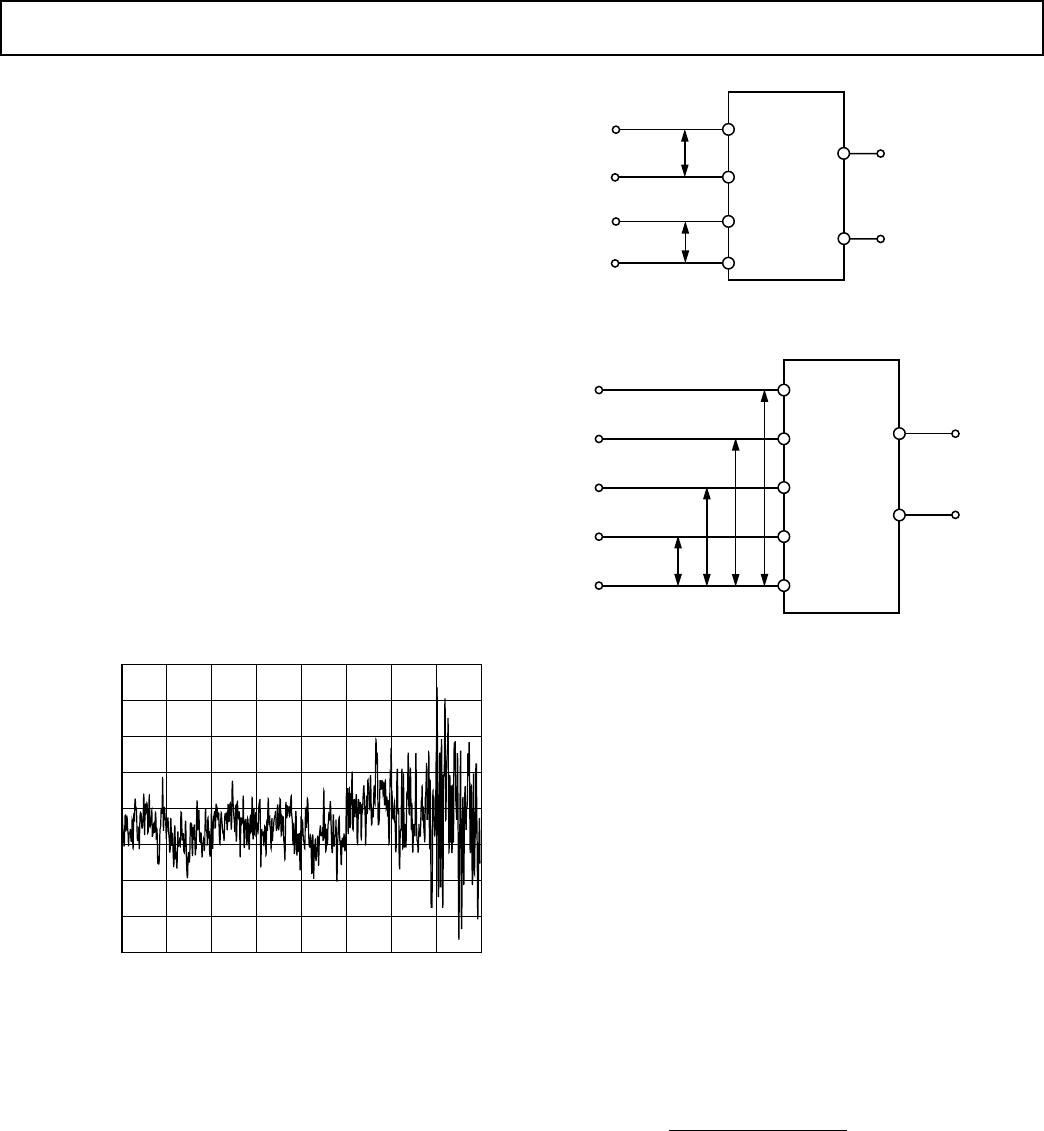
The basic connection diagram for the AD7709 is shown in
Figure 14. An AD780/REF195, precision 2.5 V reference, provides
the reference source for the part. A quartz crystal or ceramic
resonator provides the 32.768 kHz master clock source for the
part. In some cases, it will be necessary to connect capacitors on
the crystal or resonator to ensure that it does not oscillate at over-
tones
of its fundamental operating frequency. The values of
capacitors will vary depending on manufacturer specifications.
Analog Input Channels
The main ADC has five associated analog input pins (labeled
AIN1 to AIN4 and AINCOM) that can be configured as two
fully differential input channels (AIN1–AIN2 and AIN3–AIN4)
or four pseudo-differential input channels (AIN1–AINCOM,
AIN2–AINCOM, AIN3–AINCOM, and AIN4–AINCOM).
Channel selection bits CH2, CHI, and CH0 in the Configuration
Register detail the different configurations. When the analog
input
channel is switched, the settling time of the part must elapse
before a new valid word is available from the ADC.
IOUT1
AIN3/P3
AINCOM
AIN1
IOUT2
AIN4/P4
REFIN1(–)
AIN2
REFIN1(+)
REFIN2(–)
REFIN2(+)
RESET
CS
DOUT
DIN
SCLK
P2/SW2
P1/SW1
XTAL1
XTAL2
5V
CHIP
SELECT
RECEIVE
(READ)
SERIAL
CLOCK
32.768kHz
CRYSTAL
PWRGND
GND
AD780/
REF195
V
IN
V
OUT
GND
V
DD
ANALOG 5V
SUPPLY
0.1F
10F
0.1F
10F
ANALOG 5V
SUPPLY
AD7709
SERIAL DATA
(WRITE)
Figure 14. Basic Connection Diagram
The output of the ADC multiplexer feeds into a high impedance
input stage of the buffer amplifier. As a result, the ADC inputs can
handle significant source impedances and are tailored for direct
connection to external resistive-type sensors like strain gauges or
Resistance Temperature Detectors (RTDs).
The absolute input voltage range on the ADC inputs when buff-
ered (AIN1 to AIN4) is restricted to a range between GND +
100 mV and V
DD
– 100 mV. Care must be taken in setting up
the common-mode voltage and input voltage range so that these
limits are not exceeded; otherwise, there will be a degradation in
linearity and noise performance.
The absolute input voltage range on the ADC inputs when
unbuffered (AINCOM) includes the range between GND – 30 mV
to
V
DD
+ 30 mV as a result of being unbuffered. The negative abso-
lute input voltage limit does allow the possibility of monitoring
small true bipolar signals with respect to GND.
REV. A
AD7709
–23–
Programmable Gain Amplifier
The output from the buffer on the ADC is applied to the input
of the on-chip programmable gain amplifier (PGA). The PGA
can be programmed through eight different unipolar and bipolar
ranges. The PGA gain range is programmed via the range bits
in the Configuration Register. With an external 2.5 V reference
applied, the unipolar ranges are 0 mV to 20 mV, 0 mV to 40 mV,
0 mV
to 80 mV, 0 mV to 160 mV, 0 mV to 320
mV
, 0 mV to
640 mV, 0 V
to 1.28 V, and 0 to 2.56 V, while bipolar ranges
are ±20 mV,
±40 mV, ±80 mV, ±160 mV, ±320 mV, ±640
mV, ±1.28 V, and
±2.56 V.
These are the ranges that should
appear at the input to the on-chip PGA.
Typical matching across ranges is shown in Figure 15. Here, the
ADC is configured in fully differential, bipolar mode with an
external 2.5 V reference, while an analog input voltage of just
greater than 19 mV is forced on its analog inputs. The ADC
continuously converts the dc voltage at an update rate of 5.35 Hz,
i.e., SF = FFh. A total of 800 conversion results are gathered.
The first 100 results gathered with the ADC operating in the
±20 mV. The ADC range is then switched to ±40 mV and 100
more results are gathered, and so on, until the last 100 samples
are gathered with the ADC configured in the ±2.5 V range. From
Figure 15, the variation in the sample mean through each range,
i.e., the range matching, is seen to be on the order of 2 µV.
0 100 200 300 400 500 600 700 800
SAMPLE COUNT
ADC INPUT VOLTAGE – mV
19.372
19.371
19.370
19.369
19.368
19.367
19.366
19.365
19.364
ADC RANGE
20mV
40mV
80mV
160mV
320mV
640mV
1.28V
2.56V
Figure 15. ADC Range Matching
Bipolar/Unipolar Configuration
The analog inputs on the AD7709 can accept either unipolar or
bipolar input voltage ranges. Bipolar input ranges do not imply that
the part can handle negative voltages with respect to system
GND. Unipolar and bipolar signals on the AIN(+) input on
the
ADC are referenced to the voltage on the respective AIN(–)
input. AIN(+) and AIN(–) refer to the signals seen by the
modulator that come from the output of the multiplexer, as
shown
in Figures 16 and 17.
FULLY DIFFERENTIAL
FULLY DIFFERENTIAL
AIN(+)
AIN(–)
AIN1
AIN2
AIN3
AIN4
AIN1
AIN2
AIN3
AIN4
MUX
ADC CHANNEL
Figure 16. Fully Differential Mode of Operation
AIN3AIN3
AIN4AIN4
AIN1/AINCOM
PSEUDO-DIFFERENTIAL
INPUT
AIN(–)
AIN(+)
AIN1
AIN1
AIN2
AIN2
AINCOM
AINCOM
ADC CHANNEL
MUX
AIN2/AINCOM
AIN3/AINCOM
AIN4/AINCOM
PSEUDO-DIFFERENTIAL
INPUT
Figure 17. Pseudo-Differential Mode of Operation
For example, if AIN(–) is 2.5 V and the ADC is configured for
an analog input range of 0 mV to 20 mV, the input voltage range
on the AIN(+) input is 2.5 V to 2.52 V. If AIN(–) is 2.5 V and
the AD7709 is configured for an analog input range of ±1.28 V,
the analog input range on the AIN(+) input is 1.22 V to 3.78 V
(i.e., 2.5 V ±1.28 V). Bipolar or unipolar options are chosen by
programming the UNI bit in the Configuration Register. This
programs the ADC for either unipolar or bipolar operation.
Programming for either unipolar or bipolar operation does not
change any of the input signal conditioning; it simply changes
the data output coding.
Data Output Coding
When the ADC is configured for unipolar operation, the output
coding is natural (straight) binary with a zero differential input
voltage resulting in a code of 000 . . . 000, a midscale voltage
resulting in a code of 100 . . . 000, and a full-scale input voltage
resulting in a code of 111 . . . 111. The output code for any analog
input voltage on the ADC can be represented as follows:
Code
AIN GAIN
V
N
REF
=
××
()
×
()
2
1 024.
where:
AIN is the analog input voltage.
GAIN is the PGA gain, i.e., 1 on the 2.56 V range and 128 on
the 20 mV range.
N = 16.

AD7709BRUZ

Mfr. #:
Manufacturer:
Analog Devices Inc.
Description:
Analog to Digital Converters - ADC 16-Bit w/ Current Sources
Lifecycle:
New from this manufacturer.
Delivery:
DHL FedEx Ups TNT EMS
Payment:
T/T Paypal Visa MoneyGram Western Union