© Semiconductor Components Industries, LLC, 1995
August, 2018 − Rev. 31
1 Publication Order Number:
LP2950/D
LP2950, LP2951, NCV2951
100 mA, Low Power Low
Dropout Voltage Regulator
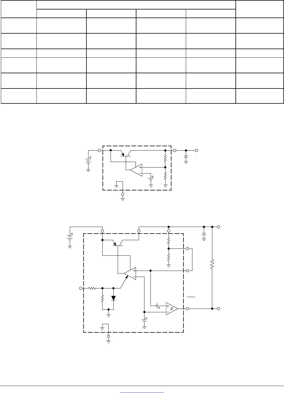
The LP2950 and LP2951 are micropower voltage regulators that are
specifically designed to maintain proper regulation with an extremely
low input−to−output voltage differential. These devices feature a very
low quiescent bias current of 75 mA and are capable of supplying
output currents in excess of 100 mA. Internal current and thermal
limiting protection is provided.
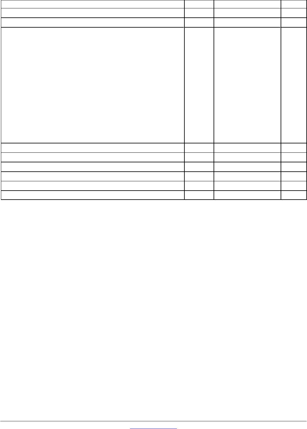
The LP2951 has three additional features. The first is the Error
Output that can be used to signal external circuitry of an out of
regulation condition, or as a microprocessor power−on reset. The
second feature allows the output voltage to be preset to 5.0 V, 3.3 V or
3.0 V output (depending on the version) or programmed from 1.25 V
to 29 V. It consists of a pinned out resistor divider along with direct
access to the Error Amplifier feedback input. The third feature is
a Shutdown input that allows a logic level signal to turn−off or turn−on
the regulator output.
Due to the low input−to−output voltage differential and bias current
specifications, these devices are ideally suited for battery powered
computer, consumer, and industrial equipment where an extension of
useful battery life is desirable. The LP2950 is available in the three
pin case 29 and DPAK packages, and the LP2951 is available in the
eight pin dual−in−line, SOIC−8 and Micro8 surface mount packages.
The ‘A’ suffix devices feature an initial output voltage tolerance
±0.5%.
Features
Low Quiescent Bias Current of 75 mA
Low Input−to−Output Voltage Differential of 50 mV at 100 mA and
380 mV at 100 mA
5.0 V, 3.3 V or 3.0 V ±0.5% Allows Use as a Regulator or Reference
Extremely Tight Line and Load Regulation
Requires Only a 1.0 mF Output Capacitor for Stability
Internal Current and Thermal Limiting
NCV Prefix for Automotive and Other Applications Requiring
Unique Site and Control Change Requirements; AEC−Q100
Qualified and PPAP Capable
These Devices are Pb−Free and RoHS Compliant
LP2951 Additional Features
Error Output Signals an Out of Regulation Condition
Output Programmable from 1.25 V to 29 V
Logic Level Shutdown Input
(See Following Page for Device Information.)
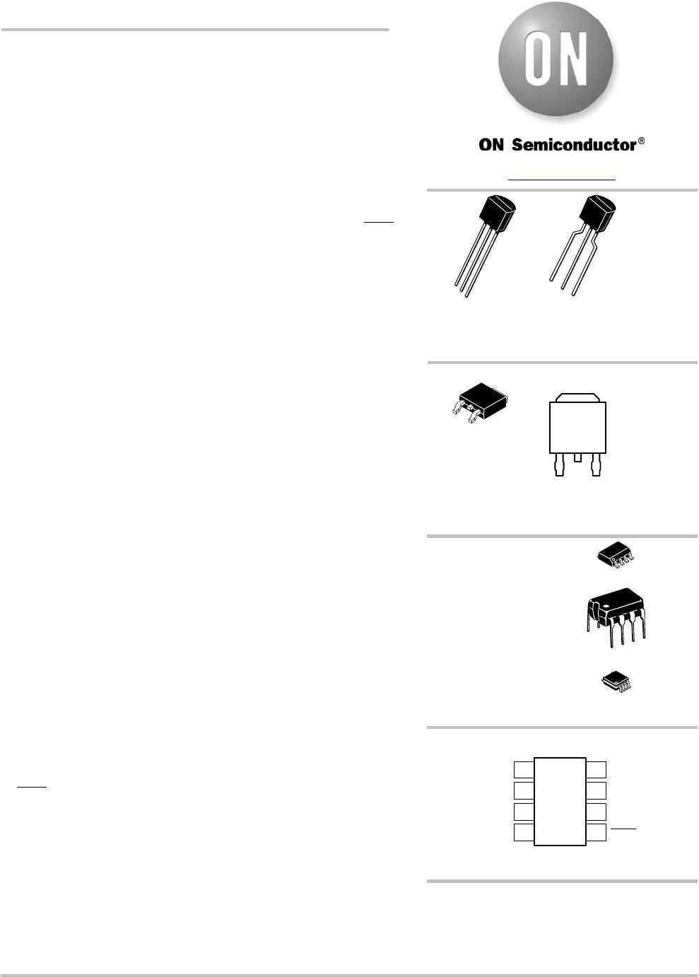
TO−92
CASE 29
See detailed ordering and shipping information in the package
dimensions section on pages 14 and 15 of this data sheet.
See general marking information in the device marking
section on page 17 of this data sheet.
ORDERING & MARKING INFORMATION
PIN CONNECTIONS
Pin: 1. Output
2. Ground
3. Input
DPAK
CASE 369C
Heatsink surface (shown as terminal 4 in
case outline drawing) is connected to Pin 2.
123
(Top View)
Pin: 1. Input
2. Ground
3. Output
8
1
8
1
8
1
PIN CONNECTIONS
18
7
6
5
2
3
4
(Top View)
Output
Sense
Shutdown
Input
Feedback
Error
Output
V
O
Tap
GND
SOIC−8
CASE 751
PDIP−8
CASE 626
Micro8E
CASE 846A
1
2
3
4
1
2
3
1
2
BENT LEAD
TAPE & REEL
AMMO PACK
STRAIGHT LEAD
BULK PACK
3
www.onsemi.com
LP2950, LP2951, NCV2951
www.onsemi.com
2
DEVICE INFORMATION
Package
Output Voltage
Operating Ambient
Temperature Range
3.0 V 3.3 V 5.0 V Adjustable
TO−92
Suffix Z
LP2950CZ−3.0
LP2950ACZ−3.0
LP2950CZ−3.3
LP2950ACZ−3.3
LP2950CZ−5.0
LP2950ACZ−5.0
Not
Available
T
A
= −40° to +125°C
DPAK
Suffix DT
LP2950CDT−3.0
LP2950ACDT−3.0
LP2950CDT−3.3
LP2950ACDT−3.3
LP2950CDT−5.0
LP2950ACDT−5.0
Not
Available
T
A
= −40° to +125°C
SOIC−8 NCV2951ACD−3.3R2 NCV2951ACDR2 NCV2951CDR2 T
A
= −40° to +125°C
SOIC−8
Suffix D
LP2951CD−3.0
LP2951ACD−3.0
LP2951CD−3.3
LP2951ACD−3.3
LP2951CD
LP2951ACD
LP2951CD
LP2951ACD
T
A
= −40° to +125°C
Micro8
Suffix DM
LP2951CDM−3.0
LP2951ACDM−3.0
LP2951CDM−3.3
LP2951ACDM−3.3
LP2951CDM
LP2951ACDM
LP2951CDM
LP2951ACDM
T
A
= −40° to +125°C
DIP−8
Suffix N
LP2951CN−3.0
LP2951ACN−3.0
LP2951CN−3.3
LP2951ACN−3.3
LP2951CN
LP2951ACN
LP2951CN
LP2951ACN
T
A
= −40° to +125°C
LP2950Cx−xx / LP2951Cxx−xx 1% Output Voltage Precision at T
A
= 25°C
LP2950ACx−xx / LP2951ACxx−xx 0.5% Output Voltage Precision at T
A
= 25°C
From
CMOS/TTL
3
Figure 1. Representative Block Diagrams
This device contains 34 active transistors.
LP2950CZ−5.0
Battery or
Unregulated DC
GND 2
Output
5.0 V/100 mA
1
Input
3
1.23 V
Reference
Error Amplifier
182 k
60 k
1.0 mF
GND 4
182 k
60 k
1.23 V
Reference
1.0 mF
LP2951CD or CN
Error
Amplifier
Battery or
Unregulated DC
Shutdown
Error
Output
5
V
O
Tap
Feedback
6
7
Input 8 Output
1
Sense 2
5.0 V/100 mA
330 k
To CMOS/TTL
75 mV/
60 mV
Error Detection
Comparator
50 k
60 k
LP2950, LP2951, NCV2951
www.onsemi.com
3
MAXIMUM RATINGS (T
A
= 25°C, unless otherwise noted.)
Rating
Symbol Value Unit
Input Voltage V
CC
30 Vdc
Peak Transient Input Voltage (t < 300 ms) V
CC
32 Vdc
Power Dissipation and Thermal Characteristics
Maximum Power Dissipation P
D
Internally Limited W
Case 751(SOIC−8) D Suffix
Thermal Resistance, Junction−to−Ambient
R
q
JA
180 °C/W
Thermal Resistance, Junction−to−Case
R
q
JC
45 °C/W
Case 369A (DPAK) DT Suffix (Note 1)
Thermal Resistance, Junction−to−Ambient
R
q
JA
92 °C/W
Thermal Resistance, Junction−to−Case
R
q
JC
6.0 °C/W
Case 29 (TO−226AA/TO−92) Z Suffix
Thermal Resistance, Junction−to−Ambient
R
q
JA
160 °C/W
Thermal Resistance, Junction−to−Case
R
q
JC
83 °C/W
Case 626 N Suffix
Thermal Resistance, Junction−to−Ambient
R
q
JA
105 °C/W
Case 846A (Micro8) DM Suffix
Thermal Resistance, Junction−to−Ambient
R
q
JA
240 °C/W
Feedback Input Voltage V
fb
−1.5 to +30 Vdc
Shutdown Input Voltage V
sd
−0.3 to +30 Vdc
Error Comparator Output Voltage V
err
−0.3 to +30 Vdc
Operating Ambient Temperature Range T
A
−40 to +125 °C
Maximum Die Junction Temperature Range T
J
+150 °C
Storage Temperature Range T
stg
−65 to +150 °C
Stresses exceeding those listed in the Maximum Ratings table may damage the device. If any of these limits are exceeded, device functionality
should not be assumed, damage may occur and reliability may be affected.

LP2950ACDT-5.0

Mfr. #:
Manufacturer:
ON Semiconductor
Description:
IC REG LINEAR 5V 100MA DPAK
Lifecycle:
New from this manufacturer.
Delivery:
DHL FedEx Ups TNT EMS
Payment:
T/T Paypal Visa MoneyGram Western Union