LP2950, LP2951, NCV2951
www.onsemi.com
10
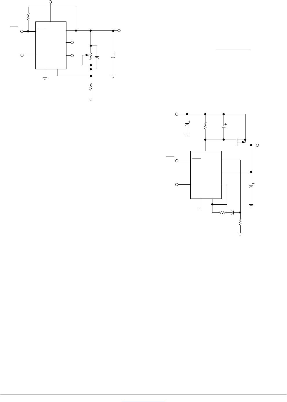
Figure 19. Adjustable Regulator
Error
Output
Shutdown
Input
V
in
V
out
1.23 to 30
V
3.3 mF
0.01 mF
NC
NC
R
2
R1
100 k
5
3
Error
SD
GND FB
47
6
V
O
T
SNS
2
V
out
V
in
8
1
The complete equation for the output voltage is:
V
out
+ V
ref
(
1 ) R1ńR2
)
) I
FB
R1
where V
ref
is the nominal 1.235 V reference voltage and I
FB
is the feedback pin bias current, nominally −20 nA. The
minimum recommended load current of 1.0 mA forces an
upper limit of 1.2 MW on the value of R2, if the regulator
must work with no load. I
FB
will produce a 2% typical error
in V
out
which may be eliminated at room temperature by
adjusting R1. For better accuracy, choosing R2
= 100 k
reduces this error to 0.17% while increasing the resistor
program current to 12 mA. Since the LP2951 typically draws
75 mA at no load with Pin 2 open circuited, the extra 12 mA
of current drawn is often a worthwhile tradeoff for
eliminating the need to set output voltage in test.
Output Noise
In many applications it is desirable to reduce the noise
present at the output. Reducing the regulator bandwidth by
increasing the size of the output capacitor is the only method
for reducing noise on the 3 lead LP2950. However,
increasing the capacitor from 1.0 mF to 220 mF only
decreases the noise from 430 mV to 160 mVrms for a 100 kHz
bandwidth at the 5.0 V output.
Noise can be reduced fourfold by a bypass capacitor
across R1, since it reduces the high frequency gain from 4
to unity. Pick
C
Bypass
[
1
2pR1 x 200 Hz
or about 0.01 mF. When doing this, the output capacitor must
be increased to 3.3 mF to maintain stability. These changes
reduce the output noise from 430 mV to 126 mVrms for a
100 kHz bandwidth at 5.0 V output. With bypass capacitor
added, noise no longer scales with output voltage so that
improvements are more dramatic at higher output voltages.
Figure 20. 1.0 A Regulator with 1.2 V Dropout
0.01 mF
10 k
MTB23P06E
1.0 mF
Unregulated
Input
Error
Output
Shutdown
Input
V
out
5.0 V ±1.0%
0 to 1.0 A
220 mF
2.0 k
5
3
Error
SD
GND FB
47
6
V
O
T
SNS
2
V
out
V
in
8
1
0.002 mF
1.0 M
LP2951CN
LP2950, LP2951, NCV2951
www.onsemi.com
11
TYPICAL APPLICATIONS
Figure 21. Lithium Ion Battery Cell Charger
1N4001
GND
4.2 V ±0.025 V
NC
NC
50 k
5
3
Error
SD
GND FB
47
6
V
O
T
SNS
2
V
out
V
in
8
1
0.1 mF
NC
LP2951CN
2.2 mF
330 pF
806 k
1.0%
2.0 M
1.0%
Lithium Ion
Rechargeable
Cell
Unregulated Input
6.0 to 10 Vdc
Figure 22. Low Drift Current Sink
Error
Output
Shutdown
Input
+V = 2.0 to 30 V
1.0 mF
R
5
3
Error
SD
GND FB
47
6
V
O
T
SNS
2
V
out
V
in
8
1
0.1 mF
Load
I
L
= 1.23/R
I
L
Figure 23. Latch Off When Error Flag Occurs
Reset
+V
in
V
out
1.0 mF
NC
NC
R2
R1
470 k
5
3
Error
SD
GND FB
47
6
V
O
T
SNS
2
V
out
V
in
8
1
LP2951CN
470 k
Error flag occurs when V
in
is too
low to maintain V
out
, or if V
out
is re-
duced by excessive load current.
Normally
Closed
2N3906
Figure 24. 5.0 V Regulator with 2.5 V Sleep Function
*Sleep
Input
+V
in
V
out
3.3 mF
NC
NC
100 k
100 k
470 k
5
3
Error
SD
GND FB
47
6
V
O
T
SNS
2
V
out
V
in
8
1
LP2951CN
200 k
100 pF
2N3906
47 k
CMOS
Gate
Error
Output
Shutdown
Input
LP2951CN
LP2950, LP2951, NCV2951
www.onsemi.com
12
330 k
Figure 25. Regulator with Early Warning and Auxiliary Output
+V
in
Memory
V+
1.0 mF
20
5
3
Error
SD
GND FB
47
6
V
O
T
SNS
2
V
out
V
in
8
1
LP2951CN
#1
1.0 mF
5
3
Error
SD
GND FB
47
6
V
O
T
SNS
2
V
out
V
in
8
1
LP2951CN
#2
NC
Reset
V
DD
mP
Early Warning
All diodes are 1N4148.
Early Warning flag on low input voltage.
Main output latches off at lower input voltages.
Battery backup on auxiliary output.
Operation: Regulator #1’s V
out
is programmed one
diode drop above 5.0 V. Its error flag becomes active
when V
in
< 5.7 V. When V
in
drops below 5.3 V, the
error flag of regulator #2 becomes active and via Q1
latches the main output “off”. When V
in
again exceeds
5.7 V, regulator #1 is back in regulation and the early
warning signal rises, unlatching regulator #2 via D3.
D4
2.7 M
Q1
2N3906
D2
D1
D3
27 k
3.6 V
NiCad
Main
Output
Figure 26. 2.0 A Low Dropout Regulator
+V
in
V
out
@ 2.0 A
100 mF
NC
NC
R2
R1
470
5
3
Error
SD
GND FB
47
6
V
O
T
SNS
2
V
out
V
in
8
1
LP2951CN
MJE2955
4.7 M
Error
Flag
V
out
= 1.25V (1.0 + R1/R2)
For 5.0 V output, use internal resistors. Wire Pin 6 to 7,
and wire Pin 2 to +V
out
Bus.
20 k
47
4.7 mF
Tant
0.05
680
0.033 mF
2N3906
10 k
Current Limit
Section
220
1000 mF
.33 mF
.01 mF
2N3906

LP2950ACDT-5.0

Mfr. #:
Manufacturer:
ON Semiconductor
Description:
IC REG LINEAR 5V 100MA DPAK
Lifecycle:
New from this manufacturer.
Delivery:
DHL FedEx Ups TNT EMS
Payment:
T/T Paypal Visa MoneyGram Western Union