LP2950, LP2951, NCV2951
www.onsemi.com
9
APPLICATIONS INFORMATION
Introduction
The LP2950/LP2951 regulators are designed with
internal current limiting and thermal shutdown making them
user−friendly. Typical application circuits for the LP2950
and LP2951 are shown in Figures 20 through 28.
These regulators are not internally compensated and thus
require a 1.0 mF (or greater) capacitance between the
LP2950/LP2951 output terminal and ground for stability.
Most types of aluminum, tantalum or multilayer ceramic
will perform adequately. Solid tantalums or appropriate
multilayer ceramic capacitors are recommended for
operation below 25°C.
At lower values of output current, less output capacitance
is required for output stability. The capacitor can be reduced
to 0.33 mF for currents less than 10 mA, or 0.1 mF for currents
below 1.0 mA. Using the 8 pin versions at voltages less than
5.0 V operates the error amplifier at lower values of gain, so
that more output capacitance is needed for stability. For the
worst case operating condition of a 100 mA load at 1.23 V
output (output Pin 1 connected to the feedback Pin 7)
a minimum capacitance of 3.3 mF is recommended.
The LP2950 will remain stable and in regulation when
operated with no output load. When setting the output
voltage of the LP2951 with external resistors, the resistance
values should be chosen to draw a minimum of 1.0 mA.
A bypass capacitor is recommended across the
LP2950/LP2951 input to ground if more than 4 inches of
wire connects the input to either a battery or power supply
filter capacitor.
Input capacitance at the LP2951 Feedback Pin 7 can
create a pole, causing instability if high value external
resistors are used to set the output voltage. Adding a 100 pF
capacitor between the Output Pin 1 and the Feedback Pin 7
and increasing the output filter capacitor to at least 3.3 mF
will stabilize the feedback loop.
Error Detection Comparator
The comparator switches to a positive logic low whenever
the LP2951 output voltage falls more than approximately
5.0% out of regulation. This value is the comparator’s
designed−in offset voltage of 60 mV divided by the 1.235 V
internal reference. As shown in the representative block
diagram. This trip level remains 5.0% below normal
regardless of the value of regulated output voltage. For
example, the error flag trip level is 4.75 V for a normal 5.0 V
regulated output, or 9.50 V for a 10 V output voltage.
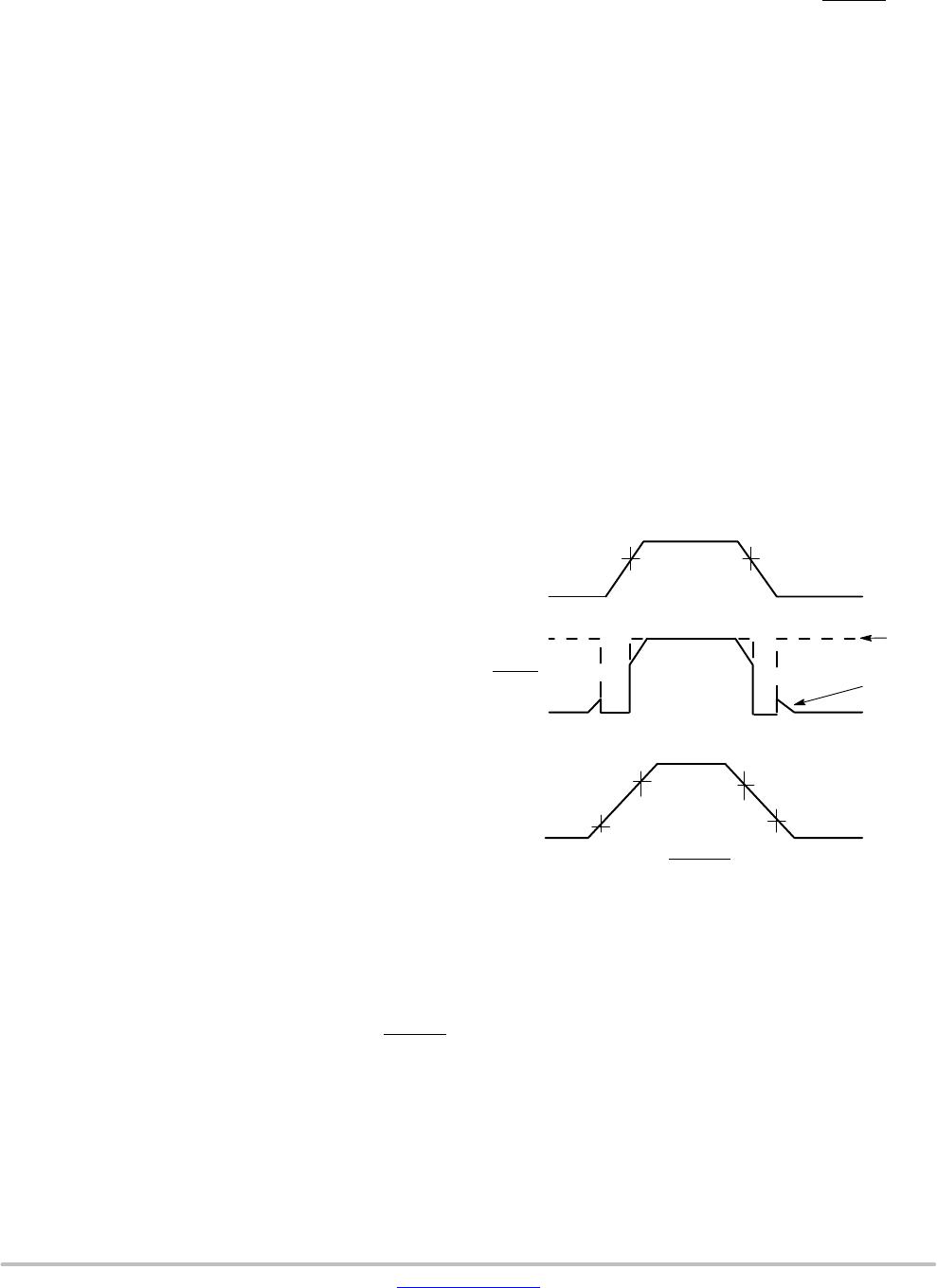
Figure 2 is a timing diagram which shows the ERROR
signal and the regulated output voltage as the input voltage
to the LP2951 is ramped up and down. The ERROR
signal
becomes valid (low) at about 1.3 V input. It goes high when
the input reaches about 5.0 V (V
out
exceeds about 4.75 V).
Since the LP2951’s dropout voltage is dependent upon the
load current (refer to the curve in the Typical Performance
Characteristics), the input voltage trip point will vary with
load current. The output voltage trip point does not vary
with load.
The error comparator output is an open collector which
requires an external pullup resistor. This resistor may be
returned to the output or some other voltage within the
system. The resistance value should be chosen to be
consistent with the 400 mA sink capability of the error
comparator. A value between 100 kW and 1.0 MW is
suggested. No pullup resistance is required if this output is
unused.
When operated in the power down mode (V
in
= 0 V),
the error comparator output will go high if it has been pulled
up to an external supply (the output transistor is in high
impedance state). To avoid this invalid response, the error
comparator output should be pulled up to V
out
(see
Figure 18).
Figure 18. ERROR Output Timing
5.0 V
4.75 V
4.70 V
4.75 V + V
dropout
4.70 V + V
dropout
1.3 V
1.3 V
Not
Valid
Pullup
to V
out
Pullup
to Ext
Output
Voltage
ERROR
Input
Voltage
Not
Valid
Programming the Output Voltage (LP2951)
The LP2951CX may be pin−strapped for the nominal
fixed output voltage using its internal voltage divider by
tying Pin 1 (output) to Pin 2 (sense) and Pin 7 (feedback) to
Pin 6 (5.0 V tap). Alternatively, it may be programmed for
any output voltage between its 1.235 reference voltage and
its 30 V maximum rating. An external pair of resistors is
required, as shown in Figure 19.