AD5246 Data Sheet
Rev. C | Page 12 of 16
I
2
C INTERFACE
Table 6. Write Mode
S 0 1 0 1 1 1 0
W
A X D6 D5 D4 D3 D2 D1 D0 A P
Slave Address Byte Data Byte
Table 7. Read Mode
S 0 1 0 1 1 1 0 R A 0 D6 D5 D4 D3 D2 D1 D0 A P
Slave Address Byte Data Byte
S = Start Condition.
P = Stop Condition.
A = Acknowledge.
X = Don’t Care.
W
= Write.
R = Read.
D6, D5, D4, D3, D2, D1, D0 = Data Bits.
t
1
t
3
t
4
t
2
t
7
t
8
t
9
P S
P
S
t
10
t
5
t
9
t
8
SCL
SDA
t
2
t
6
03875-019
Figure 26. I
2
C Interface, Detailed Timing Diagram
SCL
FRAME 1
FRAME 2
START BY
MASTER
ACK BY
AD5246
SLAVE ADDRESS BYTE
STOP BY
MASTER
DATA BYTE
SDA
0
1
0
1
1 1 0 R/W
X D6 D4 D3 D2 D1 D0
1
1 9
ACK BY
AD5246
19
D5
03875-014
Figure 27. Writing to the RDAC Register
NO ACK
BY MASTER
SCL
SDA
0
1 0 1 1 1 0 R/W
0
D6 D5 D4 D3 D2 D1 D0
1
919
FRAME 1
FRAME 2
START BY
MASTER
ACK BY
AD5246
SLAVE ADDRESS BYTE
RDAC REGISTER
STOP BY
MASTER
03875-013
Figure 28. Reading from the RDAC Register
Data Sheet AD5246
Rev. C | Page 13 of 16
OPERATION
The AD5246 is a 128-position, digitally controlled variable
resistor (VR) device.
PROGRAMMING THE VARIABLE RESISTOR
Rheostat Operation
The nominal resistance of the RDAC between Terminal A
and Terminal B is available in 5 kΩ, 10 kΩ, 50 kΩ, and 100 kΩ.
The final two or three digits of the part number determine
the nominal resistance value, that is, 10 kΩ = 10, 50 kΩ = 50.
The nominal resistance (R
AB
) of the VR has 128 contact points
accessed by the wiper terminal. The 7-bit data in the RDAC
latch is decoded to select one of the 128 possible settings.
The general equation determining the digitally programmed
output resistance between W and B is
WABWB
RR
D
DR ×+×= 2
128
)(
(1)
where:
D is the decimal equivalent of the binary code loaded in the
7-bit RDAC register.
R
AB
is the end-to-end resistance.
R
W
is the wiper resistance contributed by the on resistance
of each internal switch.
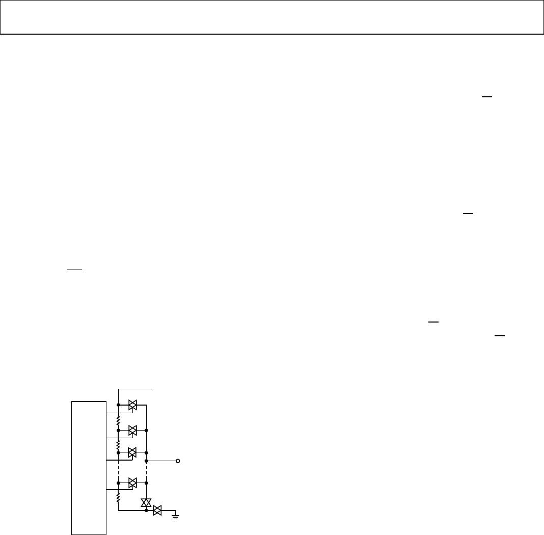
Bx
Wx
Ax
D6
D4
D5
D2
D3
D1
D0
RDAC
LATCH
AND
DECODER
R
S
R
S
R
S
03875-015
Figure 29. AD5246 Equivalent RDAC Circuit
Note that in the zero-scale condition, there is a relatively small
finite wiper resistance. Care should be taken to limit the current
flow between W and B in this state to a maximum pulse current
of no more than 20 mA. Otherwise, degradation or possible
destruction of the internal switch contact can occur.
Typical device-to-device matching is process lot dependent and
may vary by up to ±30%. Since the resistance element is proc-
essed in thin-film technology, the temperature coefficient of
R
AB
is only 45 ppm/°C.
I
2
C COMPATIBLE 2-WIRE SERIAL BUS
The first byte of the AD5246 is a slave address byte (see Table 6
and Table 7). It has a 7-bit slave address and an R/
W
bit. The
seven MSBs of the slave address are 0101110 followed by 0
for a write command or 1 to place the device in read mode.
The 2-wire I
2
C serial bus protocol operates as follows:
1. The master initiates data transfer by establishing a START
condition, which is when a high-to-low transition on the
SDA line occurs while SCL is high (see Figure 27). The
following byte is the slave address byte, which consists of
the 7-bit slave address followed by an R/
W
bit (this bit
determines whether data will be read from or written to
the slave device).
The slave whose address corresponds to the transmitted
address responds by pulling the SDA line low during the
ninth clock pulse (this is termed the acknowledge bit).
At this stage, all other devices on the bus remain idle while
the selected device waits for data to be written to or read
from its serial register. If the R/
W
bit is high, the master
reads from the slave device. Conversely, if the R/
W
bit is
low, the master writes to the slave device.
2. In write mode, after acknowledgement of the slave address
byte, the next byte is the data byte. Data is transmitted over
the serial bus in sequences of nine clock pulses (eight data
bits followed by an acknowledge bit). The transitions on
the SDA line must occur during the low period of SCL and
remain stable during the high period of SCL (see Table 6).
3. In read mode, after acknowledgment of the slave address
byte, data is received over the serial bus in sequences of
nine clock pulses (a slight difference from the write mode
where eight data bits are followed by an acknowledge bit).
Similarly, the transitions on the SDA line must occur
during the low period of SCL and remain stable during
the high period of SCL (see Figure 28).
4. When all data bits have been read or written, a STOP
condition is established by the master. A STOP condition
is defined as a low-to-high transition on the SDA line while
SCL is high. In write mode, the master pulls the SDA line
high during the tenth clock pulse to establish a STOP
condition (see Figure 27). In read mode, the master issues
a No Acknowledge for the ninth clock pulse (that is, the
SDA line remains high). The master then brings the SDA
line low before the tenth clock pulse, which goes high to
establish a STOP condition (see Figure 28).
AD5246 Data Sheet
Rev. C | Page 14 of 16
A repeated write function gives the user flexibility to update the
RDAC output a number of times after addressing the part only
once. For example, after the RDAC has acknowledged its slave
address in write mode, the RDAC output updates on each succes-
sive byte. If different instructions are needed, the write/read mode
has to start again with a new slave address and data byte.
Similarly, a repeated read function of the RDAC is also allowed.
LEVEL SHIFTING FOR BIDIRECTIONAL INTERFACE
While most legacy systems may be operated at one voltage,
a new component may be optimized at another. When two
systems operate the same signal at two different voltages, proper
level shifting is needed. For instance, one can use a 1.8 V
E
2
PROM to interface with a 5 V digital potentiometer. A level
shifting scheme is needed to enable a bidirectional communi-
cation so that the setting of the digital potentiometer can be
stored to and retrieved from the E
2
PROM. Figure 30 shows
one of the implementations. M1 and M2 can be any N channel
signal FETs, or if V
DD
falls below 2.5 V, M1 and M2 can be low
threshold FETs such as the FDV301N.
E
2
PROM
AD5246
SDA1
SCL1
D
G
R
P
R
P
1.8V
5V
S
M1
SCL2
SDA2
R
P
R
P
G
S
M2
V
DD1
= 1.8V V
DD2
=
5V
D
03875-011
Figure 30. Level Shifting for Operation at Different Potentials
ESD PROTECTION
All digital inputs are protected with a series input resistor
and parallel Zener ESD structures, as shown in Figure 31.
This applies to the digital input pins SDA and SCL.
LOGIC
340
GND
03875-002
Figure 31. ESD Protection of Digital Pins
TERMINAL VOLTAGE OPERATING RANGE
The AD5246 V
DD
and GND power supply defines the boundary
conditions for proper 3-terminal digital potentiometer
operation. Supply signals present on Terminal B and
Terminal W that exceed V
DD
or GND are clamped by
the internal forward biased diodes (see Figure 32).
B
V
DD
W
GND
03875-016
Figure 32. Maximum Terminal Voltages Set by V
DD
and GND
MAXIMUM OPERATING CURRENT
At low code values, the user should be aware that due to low
resistance values, the current through the RDAC may exceed
the 5 mA limit. In Figure 33, a 5 V supply is placed on the
wiper, and the current through Terminal W and Terminal B is
plotted with respect to code. A line is also drawn denoting the
5 mA current limit. Note that at low code values (particularly
for the 5 kΩ and 10 kΩ options), the current level increases
significantly. Care should be taken to limit the current flow
between W and B in this state to a maximum continuous
current of 5 mA and a maximum pulse current of no more than
20 mA. Otherwise, degradation or possible destruction of the
internal switch contacts can occur.
CODE (Decimal)
IWB CURRENT (mA)
0
0.01
0.1
1
10
16 32 48
64 80 96 112 128
100
5mA CURRENT LIMIT
R
AB
= 5k
R
AB
= 10k
R
AB
= 100k
R
AB
= 50k
03875-034
Figure 33. Maximum Operating Current
POWER-UP SEQUENCE
Since the ESD protection diodes limit the voltage compliance
at Terminal B and Terminal W (see Figure 32), it is important
to power V
DD
/GND before applying any voltage to Terminal B
and Terminal W; otherwise, the diode is forward biased such
that V
DD
is powered unintentionally and may affect the rest of
the user’s circuit. The ideal power-up sequence is in the follow-
ing order: GND, V
DD
, digital inputs, and then V
B
/V
W
. The
relative order of powering V
B
and V
W
and the digital inputs
is not important, providing they are powered after V
DD
/GND.

AD5246BKSZ10-RL7

Mfr. #:
Manufacturer:
Analog Devices Inc.
Description:
Digital Potentiometer ICs IC 7-Bit I2C Dig Trimmer
Lifecycle:
New from this manufacturer.
Delivery:
DHL FedEx Ups TNT EMS
Payment:
T/T Paypal Visa MoneyGram Western Union