AD5246 Data Sheet
Rev. C | Page 6 of 16
ABSOLUTE MAXIMUM RATINGS
T
A
= 25°C, unless otherwise noted.
Table 4.
Parameter Value
V
DD
to GND –0.3 V to +7 V
V
A
, V
W
to GND V
DD
Terminal Current, A–B, A–W, B–W
Pulsed
1
±20 mA
Continuous ±5 mA
Digital Inputs and Output Voltage to GND 0 V to V
DD
+ 0.3 V
Operating Temperature Range –40°C to +125°C
Maximum Junction Temperature (T
JMAX
) 150°C
Storage Temperature –65°C to +150°C
Lead Temperature (Soldering, 10 sec) 300°C
Thermal Resistance
2
θ
JA
: SC70-6 340°C/W
1
Maximum terminal current is bounded by the maximum current handling of
the switches, maximum power dissipation of the package, and maximum
applied voltage across any two of the A, B, and W terminals at a given
resistance.
2
Package power dissipation = (T
JMAX
T
A
)/θ
JA.
Stresses above those listed under Absolute Maximum Ratings
may cause permanent damage to the device. This is a stress
rating only; functional operation of the device at these or any
other conditions above those indicated in the operational
section of this specification is not implied. Exposure to absolute
maximum rating conditions for extended periods may affect
device reliability.
ESD CAUTION
ESD (electrostatic discharge) sensitive device. Electrostatic charges as high as 4000 V readily accumulate on
the human body and test equipment and can discharge without detection. Although this product features
proprietary ESD protection circuitry, permanent damage may occur on devices subjected to high energy
electrostatic discharges. Therefore, proper ESD precautions are recommended to avoid performance
degradation or loss of functionality.
Data Sheet AD5246
Rev. C | Page 7 of 16
PIN CONFIGURATION AND FUNCTION DESCRIPTIONS
V
DD
1
GND
2
SCL
3
B
6
W
5
SDA
4
AD5246
TOP VIEW
(Not to Scale)
03875-018
Figure 2. Pin Configuration
Table 5. Pin Function Descriptions
Pin No. Mnemonic Description
1 V
DD
Positive Power Supply.
2 GND Digital Ground.
3 SCL Serial Clock Input. Positive edge triggered.
4 SDA Serial Data Input/Output.
5 W W Terminal.
6 B B Terminal.
AD5246 Data Sheet
Rev. C | Page 8 of 16
TYPICAL PERFORMANCE CHARACTERISTICS
CODE (Decimal)
RHEOSTAT MODE INL (LSB)
0
–1.0
0
0.2
1.0
16 32 48 64 80 96 112 128
–0.8
–0.6
–0.4
–0.2
0.4
0.6
0.8
V
DD
= 2.7V
V
DD
= 5.5V
T
A
= 25°
C
R
AB
= 10k
RHEOSTAT MODE INL (LSB)
03875-020
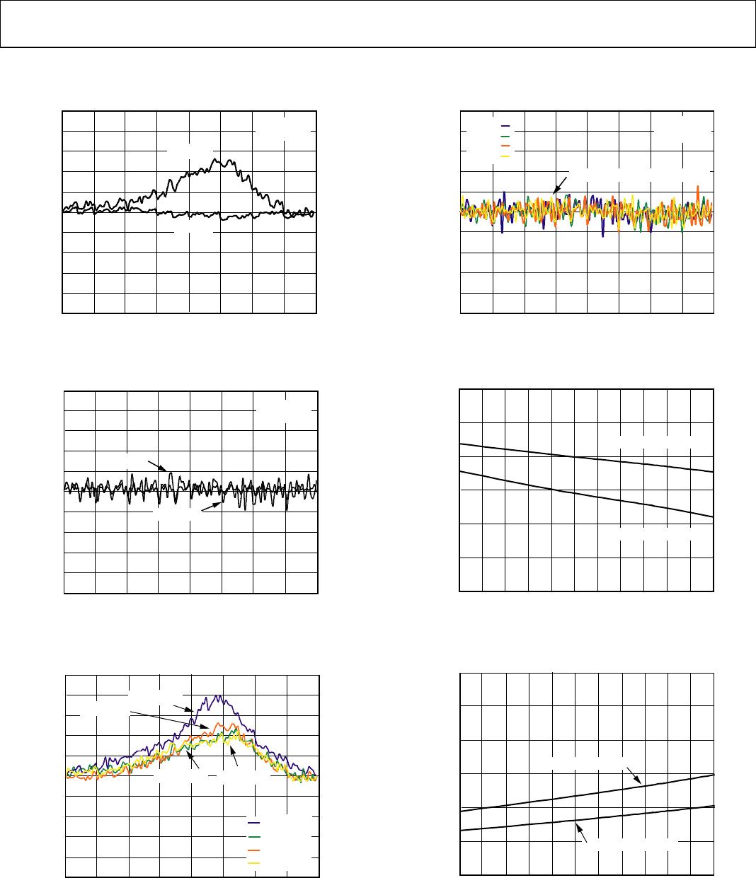
Figure 3. R-INL vs. Code vs. Supply Voltages
CODE (Decimal)
RHEOSTAT MODE DNL (LSB)
0
–0.5
–0.4
–0.3
–0.2
16 32 48
64 80 96 112 128
–0.1
0
0.1
0.2
0.3
0.4
0.5
V
DD
= 2.7V
V
DD
= 5.5V
T
A
= 25°
C
R
AB
= 10k
03875-021
Figure 4. R-DNL vs. Code vs. Supply Voltages
CODE (Decimal)
RHEOSTAT MODE INL (LSB)
0
–1.0
–0.8
–0.6
–0.4
16 32 48
–0.2
0
0.2
0.4
0.6
0.8
1.0
64 80 96 112 128
T
A
= –40°
C
T
A
= +25°
C
T
A
= +85°
C
T
A
= +125°
C
T
A
= –40°
C
T
A
= +85°
C
T
A
= +25°
C
T
A
= +125°
C
03875-022
Figure 5. R-INL vs. Code vs. Temperature
CODE (Decimal)
RHEOSTAT MODE DNL (LSB)
0
–0.5
–0.4
–0.3
–0.2
16 32 48
–0.1
0
0.1
0.2
0.3
0.4
0.5
64 80 96 112
128
T
A
= –40°
C,
+25°
C,
+85°
C,
+125°
C
–40°
C
+25°
C
+85°
C
+125°
C
V
DD
= 2.7V
R
AB
= 10k
03875-023
Figure 6. R-DNL vs. Code vs. Temperature
TEMPERATURE (°
C
)
RHEOSTAT MODE INL (LSB)
–40
–3.0
–0.5
0
–25 –10 5
20 35 50 65 80
–2.5
–2.0
–1.5
–1.0
FSE, FULL-SCALE ERROR (LSB)
95 110 125
V
DD
= 5.5V, V
A
= 5.5V
V
DD
= 2.7V, V
A
= 2.7V
03875-024
Figure 7. Full-Scale Error vs. Temperature
TEMPERATURE (
°C
)
ZSE, ZERO-SCALE ERROR (LSB)
–40
0
0.25
0.50
0.75
–25 –10 5
1.00
1.25
1.50
20 35 50 65 80 95 110 125
V
DD
= 5.5V, V
A
= 5.5V
V
DD
= 2.7V, V
A
= 2.7V
03875-025
Figure 8. Zero-Scale Error vs. Temperature

AD5246BKSZ10-RL7

Mfr. #:
Manufacturer:
Analog Devices Inc.
Description:
Digital Potentiometer ICs IC 7-Bit I2C Dig Trimmer
Lifecycle:
New from this manufacturer.
Delivery:
DHL FedEx Ups TNT EMS
Payment:
T/T Paypal Visa MoneyGram Western Union