A4973SLBTR-T

V
BB
RC
V
CC
LOGIC
SUPPLY
LOAD
SUPPLY
9
PHASE
UVLO
& TSD
R
S
MODE
REF
OUT
A
OUT
B
ENABLE
SENSE
+
BRAKE
INPUT LOGIC
GROUND
Q
R
S
PWM LATCH
V
CC
+ –
BLANKING
SLEEP &
STANDBY MODES
V
TH
R
T
C
T
1
2
2
3
6
7
8
10
11
14
15
4
GROUND
12
LOAD
SUPPLY
16
5 13
Description
Designed for bidirectional pulse width modulated (PWM)
current control of inductive loads, the A4973 is capable of
continuous output currents to ±1.5 A and operating voltages
to 50 V. Internal fixed off-time PWM current-control circuitry
can be used to regulate the maximum load current to a desired
value. The peak load current limit is set by the user’s selection
of an input reference voltage and external sensing resistor. The
fixed off-time pulse duration is set by a user- selected external
RC timing network. Internal circuit protection includes thermal
shutdown with hysteresis, transient-suppression diodes, and
crossover current protection. Special power-up sequencing is
not required.
With the ENABLE input held low, the PHASE input controls
load current polarity by selecting the appropriate source and
sink driver pair. The MODE input determines whether the
PWM current-control circuitry operates in a slow current-decay
mode (only the selected source driver switching) or in a fast
current-decay mode (selected source and sink switching). A
user-selectable blanking window prevents false triggering of
the PWM current-control circuitry. With the ENABLE input
held high, all output drivers are disabled. A sleep mode is
provided to reduce power consumption.
4973DS, Rev. 1
Features and Benefits
±1.5 A continuous output current
50 V output voltage rating
3 V to 5.5 V logic supply voltage
Internal PWM current control
Fast and slow current-decay modes
Sleep (low current consumption) mode
Internal transient-suppression diodes
Internal thermal shutdown circuitry
Crossover current and UVLO protection
Full-Bridge PWM Motor Driver
Continued on the next page…
Packages:
Functional Block Diagram
Not to scale
A4973
Package B, 16-pin DIP
with exposed tabs
Package LB, 16-pin SOIC
with internally fused pins
Full-Bridge PWM Motor Driver
A4973
2
Allegro MicroSystems, LLC
115 Northeast Cutoff
Worcester, Massachusetts 01615-0036 U.S.A.
1.508.853.5000; www.allegromicro.com
Description (continued)
Absolute Maximum Ratings
Characteristic Symbol Notes Rating Units
Load Supply Voltage V
BB
50 V
Logic Supply Voltage V
CC
6V
Logic/Reference Input Voltage Range V
IN
–0.3 to 6 V
Sense Voltage V
SENSE
0.5 V
Output Current, Continuous I
OUT
Output current rating may be limited by duty cycle, ambient
temperature, and heat sinking. Under any set of conditions, do
not exceed the speci ed current rating or a junction tempera-
ture of 150°C.
±1.5 A
Transient Output Current I
OUT
t
W
< 2 s6A
Package Power Dissipation P
D
See graph W
Operating Ambient Temperature T
A
Range S –20 to 85 ºC
Maximum Junction Temperature T
J
(max)
Fault conditions that produce excessive junction temperature
will activate the device’s thermal shutdown circuitry. These
conditions can be tolerated but should be avoided.
150 ºC
Storage Temperature T
stg
–55 to 150 ºC
Selection Guide
Part Number Package Packing
A4973SB-T 16-pin DIP with exposed thermal tabs 25 pieces per tube
A4973SLBTR-T 16-pin SOICW with internally-fused pins 1000 pieces per reel
When a logic low is applied to the BRAKE input, the braking
function is enabled. This overrides ENABLE and PHASE to turn
off both source drivers and turn on both sink drivers. The brake
function can be used to dynamically brake brush DC motors.
The A4973 is supplied in a choice of two power packages; a
16-pin dual-in-line plastic package with copper heat-sink tabs,
and a 16-pin plastic SOIC with copper heat-sink tabs. For both
package styles, the power tab is at ground potential and needs no
electrical isolation. Each package type is available in a lead (Pb)
free version (100% matte tin plated leadframe).
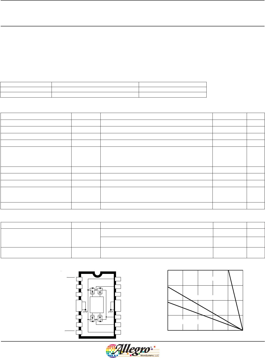
Thermal Characteristics
Characteristic Symbol Test Conditions* Value Units
Package Thermal Resistance, Junction
to Ambient
R
JA
B Package, single-layer PCB, 1 in.
2
2-oz. exposed copper 43 ºC/W
LB Package, 2-layer PCB, 0.3 in.
2
2-oz. exposed copper each
side
67 ºC/W
Package Thermal Resistance, Junction
to Tab
R
JT
6 ºC/W
*Additional thermal information available on Allegro website.
MODE
GROUND
GROUND
LOGIC
SUPPLY
PHASE
GROUND
GROUND
RC
SENSE
LOAD
SUPPLY
Dwg. PP-056
BRAKE
REF
LOAD
SUPPLY
V
CC
OUT
B
OUT
A
V
BB
V
BB
LOGIC
ENABLE
1
2
3
4
5
6
7
89
10
11
12
13
14
15
16
50 75 100 125 150
1
0
ALLOWABLE PACKAGE POWER DISSIPATION (W)
TEMPERATURE IN °C
4
3
2
25
R = 6.0°C/W
θJT
SUFFIX 'B', R = 43°C/W
θ
JA
SUFFIX 'LB', R = 67°C/W
θJA
Note the A4973SB (DIP) and
the A4973SLB (SOIC) are
electrically identical and share
a common terminal number
assignment.
Full-Bridge PWM Motor Driver
A4973
3
Allegro MicroSystems, LLC
115 Northeast Cutoff
Worcester, Massachusetts 01615-0036 U.S.A.
1.508.853.5000; www.allegromicro.com
ELECTRICAL CHARACTERISTICS at T
J
= 25°C, V
CC
= 3.0 V to 5.5 V (unless otherwise noted.)
Characteristic Symbol Test Conditions Min. Typ. Max. Unit
Power Outputs
Load Supply Voltage Range V
BB
Operating 5 50 V
Output Leakage Current I
CEX
V
OUT
= V
BB
<1.0 50 A
V
OUT
= 0 V
<–1.0 –50 A
Output On Resistance R
DS(on)
Total sink and source, I
OUT
= 1.5 A, V
BB
> 8 V, T
J
= 25°C 1 1.4
AC Timing
PWM RC Fixed Off-time t
OFF RC
C
T
= 680 pF, R
T
= 30 k, V
CC
= 3.3 V 18.3 20.4 22.5 s
PWM Minimum On Time t
ON(min)
V
CC
= 3.3 V, R
T
12 k, C
T
= 680 pF 0.8 1.4 1.9 s
V
CC
= 5.0 V, R
T
12 k, C
T
= 470 pF 0.8 1.6 2.0 s
Crossover Dead Time t
CODT
500 ns
Maximum PWM Frequency f
PWM(max)
I
OUT
= 1.5 A 70 kHz
Control Circuitry
Thermal Shutdown Temperature T
J
165 °C
Thermal Shutdown Hysteresis T
J
–15°C
UVLO Enable Threshold 2.5 2.75 3.0 V
UVLO Hysteresis 0.12 0.17 0.25 V
Logic Supply Current
I
CC(ON)
V
ENABLE
= V
IN(0)
, V
BRAKE
= V
IN(1)
2.7 3.5 mA
I
CC(Sleep)
V
ENABLE
= V
MODE
= V
BRAKE
= V
IN(1)
250 450 A
Motor Supply Current (No Load)
I
BB(ON)
V
ENABLE
= V
IN(0)
500 700 A
I
BB(Sleep)
V
ENABLE
= V
MODE
= V
BRAKE
= V
IN(1)
<1.0 3 A
Logic Supply Voltage Range V
CC
Operating 3.0 5.0 5.5 V
Logic Input Voltage
V
IN(1)
V
CC
×
0.55
––V
V
IN(0)
––
V
CC
×
0.27
V
Logic Input Current
I
IN(1)
V
IN
= V
CC
= 5 V 0 –10 A
I
IN(0)
V
IN
= 0 V, V
CC
= 5 V –106 –200 A
Reference Input Current I
REF
V
REF
= 0 V to 1 V ±5.0 A
Comparator Input Offset Volt. V
IO
V
REF
= 0 V ±2.0 ±5.0 mV
Reference Input Voltage Range V
REF
REF Pin 0 1 V
Gain V
REF
= 1 V 1.9 2 2.1

A4973SLBTR-T

Mfr. #:
Manufacturer:
Description:
Full Bridge Motor Driver 16-Pin SOIC W T/R
Lifecycle:
New from this manufacturer.
Delivery:
DHL FedEx Ups TNT EMS
Payment:
T/T Paypal Visa MoneyGram Western Union

Products related to this Datasheet