Full-Bridge PWM Motor Driver
A4973
6
Allegro MicroSystems, LLC
115 Northeast Cutoff
Worcester, Massachusetts 01615-0036 U.S.A.
1.508.853.5000; www.allegromicro.com
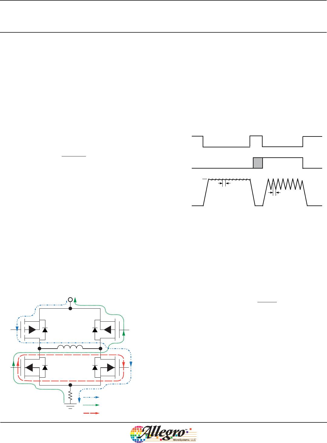
The operation of the circuit is as follows: when the PWM latch is
reset by the current comparator, the voltage on the RC terminal
will begin to decay from approximately 0.60V
CC
. When the
voltage on the RC terminal reaches approximately 0.22V
CC
, the
PWM latch is set, thereby enabling the driver(s).
RC Blanking. In addition to determining the fixed off-time of
the PWM control circuit, the C
T
component sets the comparator
blanking time. This function blanks the output of the comparator
when the outputs are switched by the internal current-control
circuitry (or by the PHASE, BRAKE, or ENABLE inputs).
The comparator output is blanked to prevent false over-current
detections due to reverse recovery currents of the clamp diodes,
and/or switching transients related to distributed capacitance in
the load.
During internal PWM operation, at the end of the t
OFF
time, the
comparator’s output is blanked and C
T
begins to be charged
from approximately 0.22V
CC
by an internal current source of
approximately 1 mA. The comparator output remains blanked
until the voltage on C
T
reaches approximately 0.60V
CC
.
When a transition of the PHASE input occurs, C
T
is discharged
to near ground during the crossover delay time (the crossover
delay time is present to prevent simultaneous conduction of
the source and sink drivers). After the crossover delay, C
T
is
charged by an internal current source of approximately 1 mA.
The comparator output remains blanked until the voltage on C
T
reaches approximately 0.60V
CC
.
When the device is disabled, via the ENABLE input, C
T
is
discharged to near ground. When the device is re-enabled, C
T
is
charged by an internal current source of approximately 1 mA.
The comparator output remains blanked until the voltage on C
T
reaches approximately 0.60V
CC
.
For 3.3 V operation, the minimum recommended value
for C
T
is 680 pF ± 5 %. For 5.0 V operation, the minimum
recommended value for C
T
is 470 pF ± 5%. These values
ensure that the blanking time is sufficient to avoid false trips
of the comparator under normal operating conditions. For
optimal regulation of the load current, the above values for C
T
are recommended and the value of R
T
can be sized to determine
t
OFF
. For more information regarding load current regulation, see
below.
LOAD CURRENT REGULATION
WITH INTERNAL PWM
CURRENT-CONTROL CIRCUITRY
When the device is operating in slow current-decay mode,
there is a limit to the lowest level that the PWM current-
control circuitry can regulate load current. The limitation is the
minimum duty cycle, which is a function of the user-selected
value of t
OFF
and the minimum on-time pulse t
ON(min)
max that
occurs each time the PWM latch is reset. If the motor is not
rotating (as in the case of a stepper motor in hold/detent mode, a
brush dc motor when stalled, or at startup), the worst case value
of current regulation can be approximated by:
{ [ V
BB
– (2 × I × R
DS
) ] × t
ON(min)
max } – [1.05 (I × R
DS
+ V
F
) × t
OFF
]
1.05 × (t
ON(min)
max + t
OFF
) × R
LOAD
I
AVE
where t
OFF
= R
T
x C
T
, R
LOAD
is the series resistance of the load,
V
BB
is the motor supply voltage and t
ON(min)
max is specified in
the Electrical Characteristics table. When the motor is rotating,
the back EMF generated will influence the above relationship.
For brush dc motor applications, the current regulation is
improved. For stepper motor applications, when the motor is
rotating, the effect is more complex. A discussion of this subject
is included in the section on stepper motors below.
The following procedure can be used to evaluate the worst-case
slow current-decay internal PWM load current regulation in the
system:
1. Set V
REF
to 0 volts. With the load connected and the PWM
current control operating in slow current-decay mode, use an
oscilloscope to measure the time the output is low (sink on) for
the output that is chopping. This is the typical minimum on time
(t
ON(min)
typ) for the device.
2. The C
T
then should be increased until the measured value
of t
ON(min)
is equal to t
ON(min)
max as specified in the electrical
characteristics table.
3. When the new value of C
T
has been set, the value of R
T
should
be decreased so the value for t
OFF
= R
T
x C
T
(with the artificially
increased value of C
T
) is equal to the nominal design value.
4. The worst-case load-current regulation then can be measured
in the system under operating conditions.