A4973SLBTR-T

Full-Bridge PWM Motor Driver
A4973
7
Allegro MicroSystems, LLC
115 Northeast Cutoff
Worcester, Massachusetts 01615-0036 U.S.A.
1.508.853.5000; www.allegromicro.com
PWM of the PHASE and ENABLE Inputs. The
PHASE and ENABLE inputs can be pulse-width modulated
to regulate load current. If the internal PWM current control is
used, the comparator blanking function is active during phase
and enable transitions. This eliminates false tripping of the
over-current comparator caused by switching transients (see RC
Blanking section, above).
Enable PWM. With the MODE input low, toggling the
ENABLE input turns on and off the selected source and sink
drivers. The corresponding pair of intrinsic flyback and ground-
clamp diodes conduct after the drivers are disabled, resulting
in fast current decay. When the device is enabled the internal
current-control circuitry will be active and can be used to limit
the load current in a slow current-decay mode.
For applications that PWM the ENABLE input and desire the
internal current-limiting circuit to function in the fast decay
mode, the ENABLE input signal should be inverted and
connected to the MODE input. This prevents the device from
being switched into sleep mode when the ENABLE input is low.
Phase PWM. Toggling the PHASE terminal selects which
sink/source pair is enabled, producing a load current that varies
with the duty cycle and remains continuous at all times. This
can have added benefits in bidirectional brush dc servo motor
applications as the transfer function between the duty cycle on
the PHASE input and the average voltage applied to the motor is
more linear than in the case of ENABLE PWM control (which
produces a discontinuous current at low current levels). For more
information see DC Motor Applications section, below.
Synchronous Fixed-Frequency PWM. The internal
PWM current-control circuitry of multiple A4973 devices can
be synchronized by using the simple circuit shown in figure 3.
A 555 IC can be used to generate the reset pulse/blanking signal
(t
1
) for the device and the period of the PWM cycle (t
2
). The
value of t
1
should be a minimum of 1.5 ms. When used in this
configuration, the R
T
and C
T
components should be omitted. The
PHASE and ENABLE inputs should not be PWMed with this
circuit configuration due to the absence of a blanking function
synchronous with their transitions.
Miscellaneous Information. A logic high applied to both
the ENABLE and MODE terminals puts the device into a sleep
mode to minimize current consumption when not in use.
An internally generated dead time prevents crossover currents
that can occur when switching phase or braking.
Thermal protection circuitry turns off all drivers should the
junction temperature reach 165°C (typical). This is intended
only to protect the device from failures due to excessive junction
temperatures and should not imply that output short circuits
are permitted. The hysteresis of the thermal shutdown circuit is
approximately 15°C.
APPLICATION NOTES
Current Sensing. The actual peak load current (I
PEAK
) will
be above the calculated value of I
TRIP
due to delays in the turn
off of the drivers. The amount of overshoot can be approximated
by:
(V
BB
– [(I
TRIP
x R
LOAD
) + V
BEMF
]) x t
PWM(OFF)
L
LOAD
I
OS
where V
BB
is the motor supply voltage, V
BEMF
is the back-EMF
voltage of the load, R
LOAD
and L
LOAD
are the resistance and
inductance of the load respectively, and t
PWM(OFF)
is specified in
the electrical characteristics table.
The reference terminal has a maximum input bias current
of ±5 μA. This current should be taken into account when
determining the impedance of the external circuit that sets the
reference voltage value.
To minimize current-sensing inaccuracies caused by ground
trace I x R drops, the current-sensing resistor should have a
separate return to the ground terminal of the device. For low-
value sense resistors, the I x R drops in the printed wiring board
can be significant and should be taken into account. The use of
sockets should be avoided as their contact resistance can cause
variations in the effective value of R
S
.
Generally, larger values of R
S
reduce the aforementioned effects
but can result in excessive heating and power loss in the sense
resistor. The selected value of R
S
should not cause the absolute
maximum voltage rating of 500 mV, for the SENSE terminal, to
be exceeded.
Dwg. EP-060
100 kΩ
20 kΩ
1N4001
2N2222
V
CC
RC
1
RC
N
t
1
2
t
Figure 3
Synchronous Fixed-Frequency Control Circuit
Full-Bridge PWM Motor Driver
A4973
8
Allegro MicroSystems, LLC
115 Northeast Cutoff
Worcester, Massachusetts 01615-0036 U.S.A.
1.508.853.5000; www.allegromicro.com
The current-sensing comparator functions down to ground
allowing the device to be used in microstepping, sinusoidal, and
other varying current-profile applications.
Thermal Considerations. For reliable operation it is
recommended that the maximum junction temperature be kept
below 110°C to 125°C. The junction temperature can be measured
best by attaching a thermocouple to the power tab/batwing of the
device and measuring the tab temperature, T
TAB
. The junction
temperature can then be approximated by using the formula:
T
J
T
TAB
+ I
2
LOAD
× R
DS(on)
x R
JT
The value for R
θJT
is given in the package thermal resistance table
for the appropriate package.
The power dissipation of the batwing packages can be improved
by 20% to 30% by adding a section of printed circuit board
copper (typically 6 to 18 square centimeters) connected to the
batwing terminals of the device.
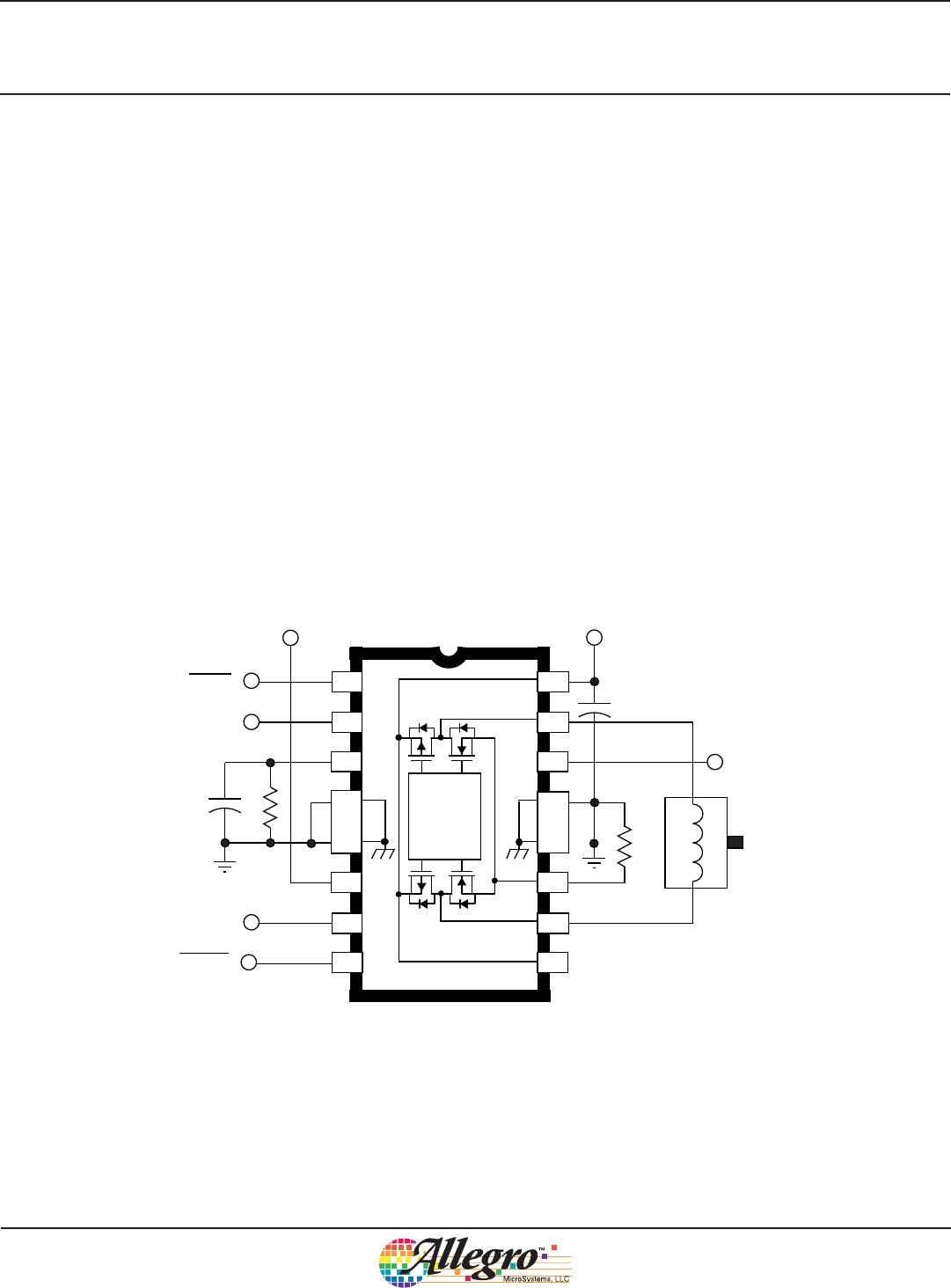
PCB Layout. The load supply terminal, V
BB
, should
be decoupled with an electrolytic capacitor (>47 μF is
recommended) placed as close to the device as is physically
practical. To minimize the effect of system ground I x R drops on
the logic and reference input signals, the system ground should
have a low-resistance return to the motor supply voltage. See also
the Current Sensing and Thermal Considerations sections, above.
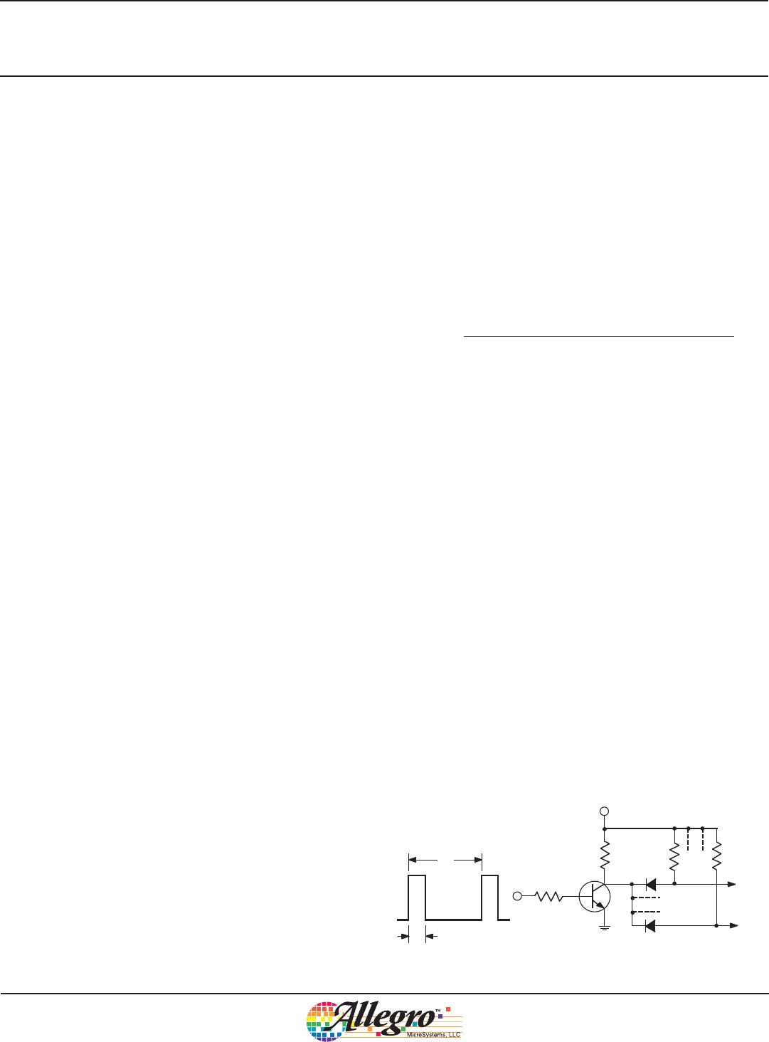
Fixed Off-Time Selection. With increasing values of t
OFF,
switching losses will decrease, low-level load-current regulation
will improve, EMI will be reduced, the PWM frequency will
decrease, and ripple current will increase. The value of t
OFF
can
be chosen for optimization of these parameters. For applications
where audible noise is a concern, typical values of t
OFF
are chosen
to be in the range of 15 to 35 μs.
Stepper Motor Applications. The MODE terminal can be
used to optimize the performance of the device in microstepping/
sinusoidal stepper-motor drive applications. When the load
current is increasing, slow decay mode is used to limit the
switching losses in the device and iron losses in the motor. This
also improves the maximum rate at which the load current can
increase (as compared to fast decay) due to the slow rate of decay
during t
OFF
. When the load current is decreasing, fast-decay mode
is used to regulate the load current to the desired level. This
prevents tailing of the current profile caused by the back-EMF
voltage of the stepper motor.
In stepper-motor applications applying a constant current to
the load, slow-decay mode PWM is typically used to limit the
switching losses in the device and iron losses in the motor.
DC Motor Applications. In closed-loop systems, the
speed of a dc motor can be controlled by PWM of the PHASE
or ENABLE inputs, or by varying the reference input voltage
(REF). In digital systems (microprocessor controlled), PWM of
the PHASE or ENABLE input is used typically thus avoiding
the need to generate a variable analog voltage reference. In this
case, a dc voltage on the REF input is used typically to limit the
maximum load current.
In dc servo applications, which require accurate positioning
at low or zero speed, PWM of the PHASE input is selected
typically. This simplifies the servo control loop because the
transfer function between the duty cycle on the PHASE input and
the average voltage applied to the motor is more linear than in the
case of ENABLE PWM control (which produces a discontinuous
current at low current levels).
With bidirectional dc servo motors, the PHASE terminal can be
used for mechanical direction control. Similar to when braking
the motor dynamically, abrupt changes in the direction of a
rotating motor produces a current generated by the back-EMF.
The current generated will depend on the mode of operation. If
the internal current control circuitry is not being used, then the
maximum load current generated can be approximated by I
LOAD
=
(V
BEMF
+ V
BB
)/R
LOAD
where V
BEMF
is proportional to the motors
speed. If the internal slow current-decay control circuitry is used,
then the maximum load current generated can be approximated
by I
LOAD
= V
BEMF
/R
LOAD
. For both cases care must be taken to
Full-Bridge PWM Motor Driver
A4973
9
Allegro MicroSystems, LLC
115 Northeast Cutoff
Worcester, Massachusetts 01615-0036 U.S.A.
1.508.853.5000; www.allegromicro.com
ensure that the maximum ratings of the device are not exceeded.
If the internal fast current-decay control circuitry is used, then the
load current will regulate to a value given by:
I
LOAD
= V
REF
/ (R
S
× 2)
CAUTION: In fast current-decay mode, when the direction of
the motor is changed abruptly, the kinetic energy stored in the
motor and load inertia will be converted into current that charges
the V
BB
supply bulk capacitance (power supply output and
decoupling capacitance). Care must be taken to ensure that the
capacitance is sufficient to absorb the energy without exceeding
the voltage rating of any devices connected to the motor supply.
See also the Brake Operation section, above.
Soldering Considerations. The lead (Pb) free (100%
matte tin) plating on lead terminations is 100% backward-
compatible for use with traditional tin-lead solders of any
composition, at any temperature of soldering that has been
traditionally used for that tin-lead solder alloy. Further, 100%
matte tin finishes solder well with tin-lead solders even at
temperatures below 232°C. This is because the matte tin dissolves
easily in the tin-lead. Additional information on soldering is
available on the Allegro Web site, www.allegromicro.com.
Figure 4 — Typical Application
V
CC
V
BB
V
BB
LOGIC
47 MF
+
1
2
3
4
5
6
7
8
9
10
11
12
13
14
15
16
30 k 7
0.5 7
V
BB
MODE
PHASE
ENABLE
BRAKE
470 pF
+5 V
REF

A4973SLBTR-T

Mfr. #:
Manufacturer:
Description:
Full Bridge Motor Driver 16-Pin SOIC W T/R
Lifecycle:
New from this manufacturer.
Delivery:
DHL FedEx Ups TNT EMS
Payment:
T/T Paypal Visa MoneyGram Western Union

Products related to this Datasheet