LT1366/LT1367
LT1368/LT1369
1
1366fb
Typical applicaTion
FeaTures DescripTion
Dual and Quad Precision
Rail-to-Rail Input and Output
Op Amps
The LT
®
1366/LT1367/LT1368/LT1369 are dual and quad
bipolar op amps which combine rail-to-rail input and output
operation with precision specifications. These op amps
maintain their characteristics over a supply range of 1.8V
to 36V. Operation is specified for 3V, 5V and ±15V supplies.
Input offset voltage is typically 150µV, with an open-loop
gain A
VOL
of 1 million while driving a 10k load. Common
mode rejection is typically 90dB over the full rail-to-rail
input range, and supply rejection is 110dB.
The LT1366/LT1367 have conventional compensation
which assures stability for capacitive loads of 1000pF or
less. The LT1368/LT1369 have compensation that requires
a 0.1µF output capacitor, which improves the amplifiers
supply rejection and reduces output impedance at high
frequencies. The output capacitors filtering action reduces
high frequency noise, which is beneficial when driving
A/D converters.
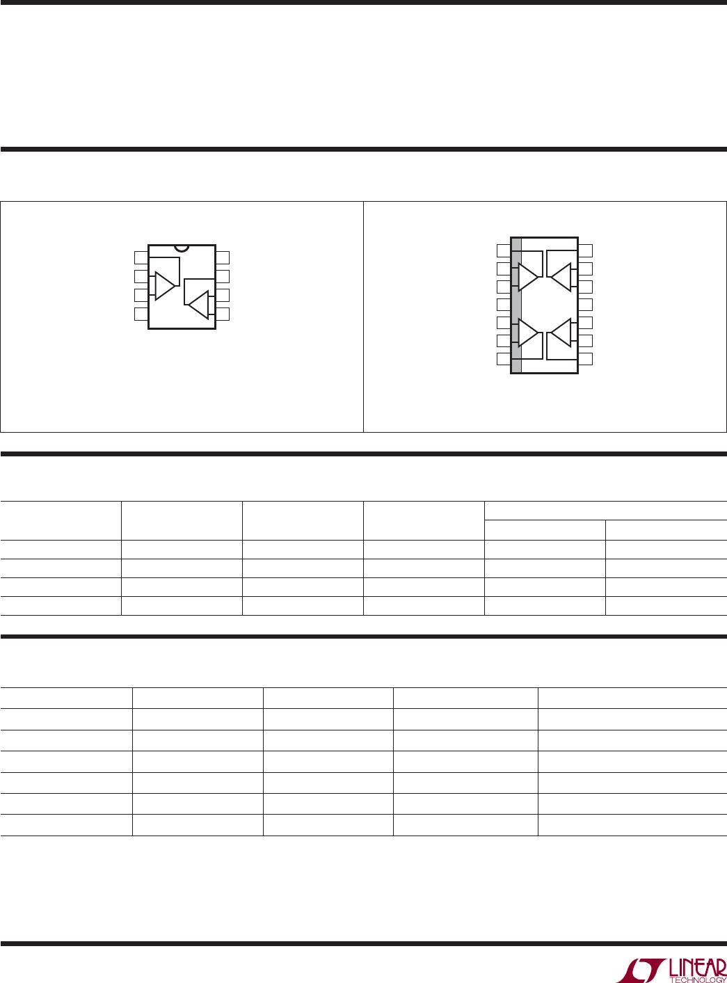
The LT1366/LT1368 are available in plastic 8-pin PDIP
and 8-lead SO packages with the standard dual op amp
pinout. The LT1367/LT1369 feature the standard quad
pinout, which is available in a plastic 14-lead SO package.
These devices can be used as plug-in replacements for
many standard op amps to improve input/output range
and precision.
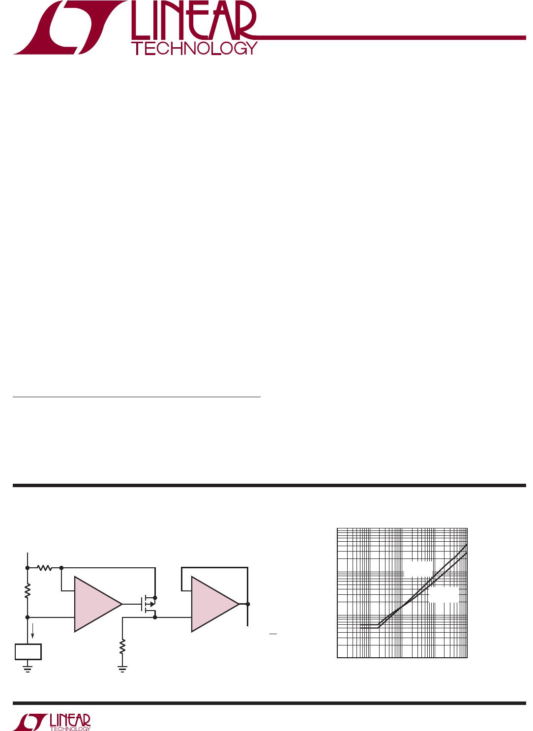
Positive Supply Rail Current Sense
applicaTions
n
Input Common Mode Range Includes Both Rails
n
Output Swings Rail-to-Rail
n
Low Input Offset Voltage: 150µV
n
High Common Mode Rejection Ratio: 90dB
n
High A
VOL
: >1V/µV Driving 10k Load
n
Low Input Bias Current: 10nA
n
Wide Supply Range: 1.8V to ±15V
n
Low Supply Current: 375µA per Amplifier
n
High Output Drive: 30mA
n
400kHz Gain-Bandwidth Product
n
Slew Rate: 0.13V/µs
n
Stable for Capacitive Loads Up to 1000pF
n
Rail-to-Rail Buffer Amplifiers
n
Low Voltage Signal Processing
n
Supply Current Sensing at Either Rail
n
Driving A/D Converters
L, LT, LTC, LTM, Over-The-Top, Linear Technology and the Linear logo are registered
trademarks and C-Load is a trademark of Linear Technology Corporation. All other trademarks
are the property of their respective owners.
LOAD CURRENT (mA)
SATURATION VOLTAGE (mV)
|V
OUT
– V
S
|
0.001 0.1 1 10
1366 TA02
0.01
1000
100
10
1
POSITIVE
RAIL
NEGATIVE
RAIL
Output Saturation Voltage vs Load Current
+
1/2 LT1366
R1
200Ω
1366 TA01
LOAD
I
LOAD
R
s
0.2Ω
R2
20k
Q1
TP0610L
V
CC
V
O
= I
LOAD
• R
S
= I
LOAD
• 20Ω
(
)
+
1/2 LT1366
R2
R1
LT1366/LT1367
LT1368/LT1369
2
1366fb
pin conFiguraTion
absoluTe MaxiMuM raTings
Total Supply Voltage (V
+
to V
) ................................ 36V
Input Current ....................................................... ±15mA
Output Short-Circuit Duration (Note 2) ........ Continuous
Operating Temperature Range ..............40°C to 85°C
(Note 1)
orDer inForMaTion
LEAD FREE FINISH TAPE AND REEL PART MARKING PACKAGE DESCRIPTION SPECIFIED TEMPERATURE RANGE
LT1366CN8#PBF LT1366CN8#TRPBF 1366 8-Lead PDIP 0°C to 70°C
LT1366CS8#PBF LT1366CS8#TRPBF 1366 8-Lead Plastic S0 0°C to 70°C
LT1367CS#PBF LT1367CS#TRPBF LT1367CS 14-Lead Plastic S0 0°C to 70°C
LT1368CN8#PBF LT1368CN8#TRPBF 1368 8-Lead PDIP 0°C to 70°C
LT1368CS8#PBF LT1368CS8#TRPBF 1368 8-Lead Plastic S0 0°C to 70°C
LT1369CS#PBF LT1369CS#TRPBF LT1369CS 14-Lead Plastic S0 0°C to 70°C
Consult LTC Marketing for parts specified with wider operating temperature ranges.
Consult LTC Marketing for information on non-standard lead based finish parts.
For more information on lead free part marking, go to: http://www.linear.com/leadfree/
For more information on tape and reel specifications, go to: http://www.linear.com/tapeandreel/
LT1366/LT1368 LT1367/LT1369
1
2
3
4
8
7
6
5
TOP VIEW
OUT A
–IN A
+IN A
V
V
+
OUT B
–IN B
+IN B
N8 PACKAGE
8-LEAD PDIP
S8 PACKAGE
8-LEAD PLASTIC SO
A
B
T
JMAX
= 150°C, θ
JA
= 130°C/W (N8)
T
JMAX
= 150°C, θ
JA
= 190°C/W (S8)
TOP VIEW
S PACKAGE
14-LEAD PLASTIC SO
1
2
3
4
5
6
7
14
13
12
11
10
9
8
OUT A
–IN A
+IN A
V
+
+IN B
–IN B
OUT B
OUT D
–IN D
+IN D
V
+IN C
– IN C
OUT C
A
B
D
C
T
JMAX
= 150°C, θ
JA
= 150°C/W
Specified Temperature Range ...................... 0°C to 70°C
Junction Temperature ......................................... 150°C
Storage Temperature Range ................. 65°C to 150°C
Lead Temperature (Soldering, 10 sec).................. 300°C
aVailable opTions
PRODUCT NUMBER NUMBER OF OP AMPS LOAD CAPACITANCE
MAX V
OS
(25°C)
AT V
S
= 5V, 0V
ORDER PART NUMBER
PLASTIC (N) SURFACE MOUNT(S)
LT1366 2 0pF < C
L
< 1000pF 475µV LT1366CN8 LT1366CS8
LT1367 4 0pF < C
L
< 1000pF 800µV LT1367CS
LT1368 2 C
L
= 0.1µF 475µV LT1368CN8 LT1368CS8
LT1369 4 C
L
= 0.1µF 800µV LT1369CS
LT1366/LT1367
LT1368/LT1369
3
1366fb
elecTrical characTerisTics
T
A
= 25°C; V
S
= 5V, 0V; V
CM
= 2.5V; V
O
= 2.5V, unless otherwise noted.
SYMBOL PARAMETER CONDITIONS MIN TYP MAX UNITS
V
OS
Input Offset Voltage (LT1366/LT1368) V
CM
= V
CC
V
CM
= V
EE
150
150
475
475
µV
µV
Input Offset Voltage (LT1367/LT1369) V
CM
= V
CC
V
CM
= V
EE
150
150
800
700
µV
µV
V
OS
Input Offset Voltage Shift (LT1366/LT1368)
Input Offset Voltage Match (Channel to Channel)
V
CM
= V
EE
to V
CC
V
CM
= V
EE
, V
CC
(Notes 4, 5)
150
250
400
700
µV
µV
Input Offset Voltage Shift (LT1367/LT1369)
Input Offset Voltage Match (Channel to Channel)
V
CM
= V
EE
to V
CC
V
CM
= V
EE
, V
CC
(Notes 4, 5)
150
250
650
1600
µV
µV
I
B
Input Bias Current V
CM
= V
CC
V
CM
= V
EE
0
–35
10
–10
35
0
nA
nA
I
B
Input Bias Current Shift V
CM
= V
EE
to V
CC
20 70 nA
I
OS
Input Offset Current V
CM
= V
CC
V
CM
= V
EE
1
0.3
12
12
nA
nA
I
OS
Input Offset Current Shift V
CM
= V
EE
to V
CC
1 12 nA
Input Bias Current Match (Channel to Channel) V
CM
= V
CC
(Note 4)
V
CM
= V
EE
(Note 4)
0
0
1
1
12
12
nA
nA
e
n
Input Noise Voltage Density f = 1kHz 29 nV/√Hz
i
n
Input Noise Current Density f = 1kHz 0.07 pA/√Hz
C
IN
Input Capacitance 12 pF
A
VOL
Large-Signal Voltage Gain V
O
= 50mV to 4.8V, R
L
= 10k 250 2000 V/mV
CMRR Common Mode Rejection Ratio (LT1366/LT1368)
CMRR Match (Channel to Channel)
V
CM
= V
EE
to V
CC
V
CM
= V
EE
to V
CC
(Note 4)
81
75
90
90
dB
dB
Common Mode Rejection Ratio (LT1367/LT1369)
CMRR Match (Channel to Channel)
V
CM
= V
EE
to V
CC
V
CM
= V
EE
to V
CC
(Note 4)
77
71
90
90
dB
dB
PSRR Power Supply Rejection Ratio
PSRR Match (Channel to Channel) (Note 4)
V
S
= 2.0V to 12V, V
CM
= V
O
= 0.5V
V
S
= 2.0V to 12V, V
CM
= V
O
= 0.5V
90
84
105
100
dB
dB
V
OL
Output Voltage Swing Low No Load
I
SINK
= 0.5mA
I
SINK
= 2.5mA
6
40
110
12
70
200
mV
mV
mV
V
OH
Output Voltage Swing High No Load
I
SINK
= 0.5mA
I
SINK
= 2.5mA
V
CC
– 0.012
V
CC
– 0.100
V
CC
– 0.250
V
CC
– 0.004
V
CC
– 0.050
V
CC
– 0.150
V
V
V
I
SC
Short-Circuit Current (Note 2) ±15 ±30 mA
I
S
Supply Current per Amplifier 340 520 µA
GBW Gain-Bandwidth Product (LT1366/LT1367)
Gain-Bandwidth Product (LT1368/LT1369)
A
V
= 1000
A
V
= 1000
0.4
0.16
MHz
MHz
t
S
Settling Time (LT1366/LT1367) A
V
= 1, V
STEP
= 4V to 0.1% 30 µs

LT1367CS#TRPBF

Mfr. #:
Manufacturer:
Analog Devices Inc.
Description:
Operational Amplifiers - Op Amps 4x Prec R2R In & Out Op Amps
Lifecycle:
New from this manufacturer.
Delivery:
DHL FedEx Ups TNT EMS
Payment:
T/T Paypal Visa MoneyGram Western Union