LT1366/LT1367
LT1368/LT1369
13
1366fb
applicaTions inForMaTion
Improved Supply Rejection in the LT1368/LT1369
The LT1368/LT1369 are variations of the LT1366/LT1367
offering greater supply rejection and lower high frequency
output impedance. The LT1368/LT1369 require a 0.1µF load
capacitance for compensation. The output capacitance
forms a filter, which reduces pickup from the supply and
lowers the output impedance. This additional filtering is
helpful in mixed analog/digital systems with common sup-
plies, or systems employing switching supplies. Filtering
also reduces high frequency noise, which may be beneficial
when driving A/D converters.
Figure 4 shows the outputs of the LT1366/LT1368 perturbed
by a 200mV
P-P
50kHz square wave added to the positive
supply. The LT1368’s power supply rejection is about ten
times greater than that of the LT1366 at 50kHz. Note the
5-to-1 scale change in the output voltage traces.
The tolerance of the external compensation capacitor is
not critical. The plots of Overshoot vs Load Current in the
Typical Performance Characteristics section illustrate the
effect of a capacitive load.
2µs/DIV
V
OUT
100mV/DIV
V
+
(AC)
100mV/DIV
LT1366 F04a
2µs/DIV
V
OUT
20mV/DIV
V
+
(AC)
100mV/DIV
LT1366 F04b
Figure 4a. LT1366 Power Supply Rejection Test Figure 4b. LT1368 Power Supply Rejection Test
Typical applicaTions
Buffering A/D Converters
Figure 5 shows the LT1368 driving an LTC
®
1288 2-chan-
nel micropower A/D converter (ADC). The LTC1288 can
accommodate voltage references and input signals equal
to the supply rails. The sampling nature of this ADC
eliminates the need for an external sample-and-hold, but
may call for a drive amplifier because of the ADC’s 12µs
settling requirement. The LT1368’s rail-to-rail operation
and low input offset voltage make it well-suited for low
power, low frequency A/D applications. Either the LT1366
or LT1368 could be used for this application. However,
for low frequencies (f < 1kHz) the LT1368 provides better
supply rejection.
CS/SHDN
CH0
CH1
GND
V
CC
(REF)
CLK
D
OUT
D
IN
LTC1288
+
+
TO µP
1µF
0.1µF
0.1µF
V
CC
V
0
V
1
1/2 LT1368
1/2 LT1368
0.1µF
LT1366 FO5
Figure 5. 2-Channel Low Power A/D Converter
LT1366/LT1367
LT1368/LT1369
14
1366fb
Precision Low Dropout Regulator
Microprocessors and complex digital circuits frequently
specify tight control of power supply characteristics. The
circuit shown in Figure 6 provides a precise 3.6V, 1A output
from a minimum 3.8V input voltage. The circuit’s nominal
operating voltage is 4.75V ±5%. The voltage reference
and resistor ratios determine output voltage accuracy,
while the LT1366’s high gain enforces 0.2% line and load
regulation. Quiescent current is about 1mA and does not
change appreciably with supply or load. All components
are available in surface mount packages.
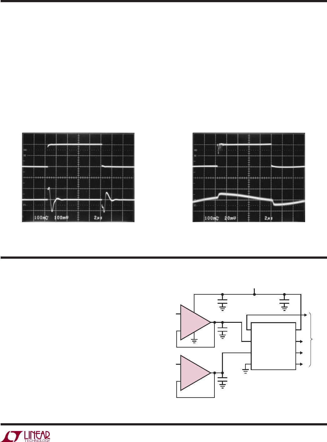
The regulators main loop consists of A1 and a logic-level
FET, Q1. The output is fed back to the op amp’s positive
input because of the phase inversion through Q1. The
regulators frequency response is limited by Q1’s roll-off
and the phase lead introduced by the output capacitors
effective series resistance (ESR). Two pole-zero networks
compensate for these effects. The pole formed with R5
and C2 rolls off the gain set with the feedback network,
while the pole formed with R7 and C3 rolls off A1’s gain
directly, which is the dominant influence on settling time.
The zeros formed with R6 and C2, and R8 and C3 provide
phase boost near the unity-gain crossover, which increases
Typical applicaTions
the regulators phase margin. Although not directly part
of the compensation, R9 decouples the op amp’s output
from Q1’s large gate capacitance.
A second loop provides a foldback current limit. A2 com-
pares the sense voltage across R1 with 50mV referenced
to the positive rail. When the sense voltage exceeds the
reference, A2’s output drives Q1’s gate positive via A1.
In current limit, the output voltage collapses and the
current limit LED (D1) turns on causing about 30mV to
drop across R3. A2 regulates Q1’s drain current so that
the deficit between the 50mV reference and the voltage
across R3 is made up across the sense resistor. The
reduced sense voltage is 20mV, which sets the current
limit to about 400mA. As the supply voltage increases, the
voltage across R3 increases, and the current limit folds
back to a lower level. The current limit loop deactivates
when the load current drops below the regulated output
current. When the supply turns on rapidly, C1 bypasses
the fold back circuit allowing the regulator to start-up into
a heavy load.
Q1 does not require a heat sink. When mounted on a type
FR4 PC board, Q1 has a thermal resistance of 50°C/W. At
1.4W worst-case dissipation, Q1 can operate up to 80°C.
C5
47µF
C4
1µF
C1
10µF
C3
6.8nF
R2
2k
R7
13k
R8
2k
R1
0.05Ω
R3
20Ω
R9
100Ω
V
IN
= 4.75V ±5%
R4
10k
D1
1.5k
Q1
Si9433DY
10k
38.5k*
D2
1N4148
5k
LT1004-1.2
R5*
20k
C2
6.8nF
R6
6.2k
R
MIN
**
1k
C
LOAD
10µF
V
OUT
3.6V
1A
Q2
2N3904
23.2k
4.75V TO 3.6V LDO AT 1A
1% METAL FILM
SET R
MIN
BASED ON LOAD CHARACTERISTICS
*
**
+
+
+
50mV
A1
1/2 LT1366
A2
1/2 LT1366
0.1µF
LT1366 F06
+
+
+
Figure 6. Precision 3.6V, 1A Low Dropout Regulator
LT1366/LT1367
LT1368/LT1369
15
1366fb
Typical applicaTions
High Side Current Source
The wide compliance current source shown in Figure 7
takes advantage of the LT1366’s ability to measure small
signals near the positive supply rail. The LT1366 adjusts
Q1’s gate voltage to force the voltage across the sense
resistor (R
SENSE
) to equal the voltage from the supply to
the potentiometers wiper. A rail-to-rail op amp is needed
because the voltage across the sense resistor must drop
to zero when the divided reference voltage is set to zero.
Q2 acts as a constant current sink to minimize error in the
reference voltage when the supply voltage varies.
The circuit can operate over a wide supply range
(5V < V
CC
< 30V). At low input voltage, circuit operation
is limited by the MOSFETs gate drive requirements. At
high input voltage, circuit operation is limited by the
LT1366’s absolute maximum ratings and the output power
requirements.
The circuit delivers 1A at 200mV of sense voltage. With a
5V input supply, the power dissipation is 5W. For opera-
tion at 70°C ambient temperature, the MOSFETs heat sink
must have a thermal resistance of:
θ
HS
= θ
JA(SYSTEM)
θ
JC(FET)
= (125°C – 70°C)/5W – 1.25°C/W
= 11°C/W –1.25°C/W
= 9.75°C/W
which is easily achievable with a small heat sink. Input
voltages greater than 5V require the use of a larger heat
sink or a reduction of the output current.
The circuit’s supply regulation is about 0.03%/V. The output
impedance is equal to the MOSFETs output impedance
multiplied by the op amp’s open-loop gain. Degradations in
current-source compliance occur when the voltage across
the MOSFETs on-resistance and the sense resistor drops
below the voltage required to maintain the desired output
current. This condition occurs when:
[V
CC
– V
OUT
] < [I
LOAD
• (R
SENSE
+ R
ON
)]
Single Supply, 1kHz, 4th Order Butterworth Filter
An LT1367 is used in Figure 8 to form a 4th order But-
terworth filter. The filter is a simplified state variable ar-
chitecture consisting of two cascaded 2nd order sections.
Each section uses the 360 degree phase shift around
+
1/2 LT1366
1k
R
SENSE
0.2Ω
40k
Q1
MTP23P06
I
LOAD
5V < V
CC
< 30V
0A < I
LOAD
< 1A AT V
CC
= 5V
0mA < I
LOAD
< 160mA AT V
CC
= 30V
Q2
2N4340
V
CC
100Ω
0.0033µF
LT1004-1.2
R
P
10k
LT1366 F07
10,000pF
10,000pF
C2
10,000pF
C1
10,000pF
R1*
29.5k
R2*
8.6k
29.5k*
11.8k*
21.5k*
11.8k*
1µF
10k
10k
V
OUT
V
IN
3.3V
+
+
+
+
A1
1/4 LT1367
A2
1/4 LT1367
A3
1/4 LT1367
A4
1/4 LT1367
LT1366 F08
*1% RESISTORS
Figure 7. High Side Current Source
Figure 8. 4-Pole 1kHz, 3.3V Single Supply, State Variable Filter Using the LT1367

LT1367CS#TRPBF

Mfr. #:
Manufacturer:
Analog Devices Inc.
Description:
Operational Amplifiers - Op Amps 4x Prec R2R In & Out Op Amps
Lifecycle:
New from this manufacturer.
Delivery:
DHL FedEx Ups TNT EMS
Payment:
T/T Paypal Visa MoneyGram Western Union