1
LT1168
1168fa
Low Power, Single
Resistor Gain Programmable,
Precision Instrumentation Amplifier
The LT
®
1168 is a micropower, precision instrumentation am-
plifier that requires only one external resistor to set gains of
1 to 10,000. The low voltage noise of 10nV/Hz (at 1kHz) is
not compromised by low power dissipation (350µA typical for
±15V supplies). The wide supply range of ±2.3V to ±18V allows
the LT1168 to fit into a wide variety of industrial as well as
battery-powered applications.
The high accuracy of the LT1168 is due to a 20ppm maximum
nonlinearity and 0.4% max gain error (G = 10). Previous mono-
lithic instrumentation amps cannot handle a 2k load resistor
whereas the nonlinearity of the LT1168 is specified for loads
as low as 2k. The LT1168 is laser trimmed for very low input
offset voltage (40µV max), drift (0.3µV/°C), high CMRR (90dB,
G = 1) and PSRR (103dB, G = 1). Low input bias currents of
250pA max are achieved with the use of superbeta process-
ing. The output can handle capacitive loads up to 1000pF in
any gain configuration while the inputs are ESD protected up
to 13kV (human body). The LT1168 with two external 5k
resistors passes the IEC 1000-4-2 level 4 specification.
The LT1168 is a pin-for-pin improved second source for the
AD620 and INA118. The LT1168, offered in 8-pin PDIP and
SO packages, requires significantly less PC board area than
discrete op amp resistor designs. These advantages make
the LT1168 the most cost effective solution for precision
instrumentation amplifier applications.
Supply Current: 530µA Max
Meets IEC 1000-4-2 Level 4 (±15kV) ESD Tests
with Two External 5k Resistors
Single Gain Set Resistor: G = 1 to 10,000
Gain Error: G = 10, 0.4% Max
Input Offset Voltage Drift: 0.3µV/°C Max
Gain Nonlinearity: G = 10, 20ppm Max
Input Offset Voltage: 40µV Max
Input Bias Current: 250pA Max
PSRR at A
V
=1: 103dB Min
CMRR at A
V
= 1: 90dB Min
Wide Supply Range: ±2.3V to ±18V
1kHz Voltage Noise: 10nV/Hz
0.1Hz to 10Hz Noise: 0.28µV
P-P
Available in 8-Pin PDIP and SO Packages
Bridge Amplifiers
Strain Gauge Amplifiers
Thermocouple Amplifiers
Differential to Single-Ended Converters
Differential Voltage to Current Converters
Data Acquisition
Battery-Powered and Portable Equipment
Medical Instrumentation
Scales
Single Supply* Pressure Monitor
NONLINEARITY (100ppm/DIV)
G = 1000 OUTPUT VOLTAGE (2V/DIV)
1168 TA01a
R
L
= 2k
V
OUT
= ± 10V
Gain Nonlinearity
*See Theory of Operation section
FEATURES
DESCRIPTIO
U
APPLICATIO S
U
TYPICAL APPLICATIO
U
+
2
3
2
1
1
1
1/2
LT1112
3.5k
5V
3.5k
3.5k
3.5k
8
7
6
1168 TA01
5
40k
20k
40k
DIGITAL
DATA
OUTPUT
4
R1
G = 200
249
3
REF
IN
AGND
ADC
LTC
®
1286
BI TECHNOLOGIES
67-8-3 R40KQ, (0.02% RATIO MATCH)
+
LT1168
, LT, LTC and LTM are registered trademarks of Linear Technology Corporation.
All other trademarks are the property of their respective owners.
2
LT1168
1168fa
Supply Voltage ...................................................... ±20V
Differential Input Voltage (Within the
Supply Voltage) ..................................................... ±40V
Input Voltage (Equal to Supply Voltage) ................ ±20V
Input Current (Note 2) ....................................... ±20mA
Output Short-Circuit Duration (Note 3) ............ Indefinite
Operating Temperature Range (Note 4) .. 40°C to 85°C
Specified Temperature Range
LT1168AC/LT1168C (Note 5) ............. 40°C to 85°C
LT1168AI/LT1168I ............................. 40°C to 85°C
Storage Temperature Range ................. 65°C to 150°C
Lead Temperature (Soldering, 10 sec).................. 300°C
ORDER PART
NUMBER
S8 PART MARKING
LT1168ACN8
LT1168ACS8
LT1168AIN8
LT1168AIS8
LT1168CN8
LT1168CS8
LT1168IN8
LT1168IS8
1168A
1168AI
T
JMAX
= 150°C, θ
JA
= 150°C/ W (N8)
T
JMAX
= 150°C, θ
JA
= 190°C/ W (S8)
T
A
= 25°C. V
S
= ±15V, V
CM
= 0V, R
L
= 10k unless otherwise noted.
1168
1168I
(Note 1)
ABSOLUTE AXI U RATI GS
WWWU
PACKAGE/ORDER I FOR ATIO
UU
W
1
2
3
4
8
7
6
5
TOP VIEW
R
G
–IN
+IN
–V
S
R
G
+V
S
OUTPUT
REF
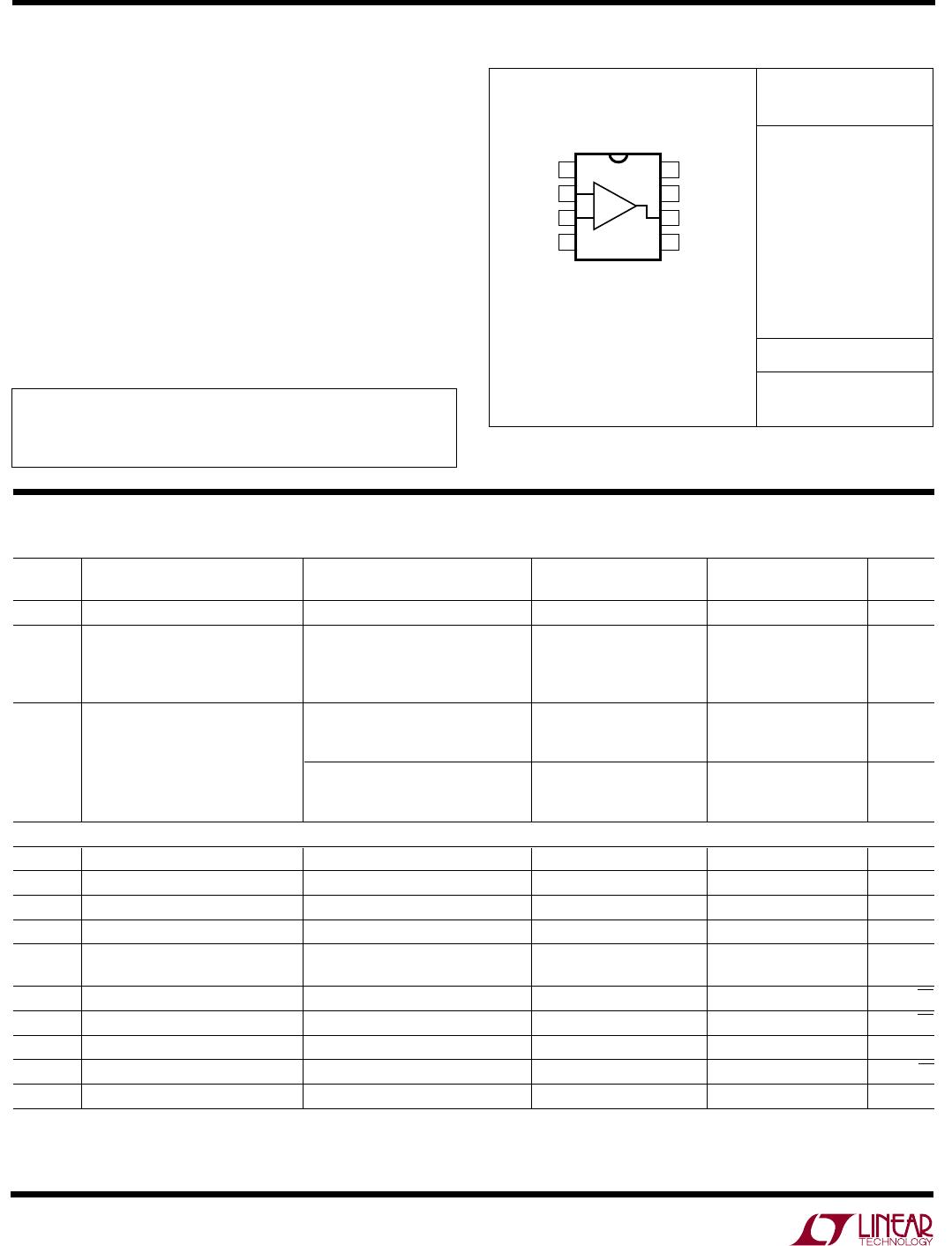
N8 PACKAGE
8-LEAD PDIP
S8 PACKAGE
8-LEAD PLASTIC SO
+
ELECTRICAL CHARACTERISTICS
Consult LTC Marketing for parts specified with wider operating temperature
ranges.
Order Options Tape and Reel: Add #TR
Lead Free: Add #PBF Lead Free Tape and Reel: Add #TRPBF
Lead Free Part Marking: http://www.linear.com/leadfree/
LT1168AC/LT1168AI LT1168C/LT1168I
SYMBOL PARAMETER CONDITIONS (Note 6) MIN TYP MAX MIN TYP MAX UNITS
G Gain Range G = 1 + (49.4k/R
G
) 1 10k 1 10k
Gain Error G = 1 0.008 0.02 0.015 0.03 %
G = 10 (Note 7) 0.04 0.4 0.05 0.5 %
G = 100 (Note 7) 0.04 0.5 0.05 0.6 %
G = 1000 (Note 7) 0.08 0.5 0.08 0.6 %
Gain Nonlinearity (Notes 7, 8) V
O
= ±10V, G = 1 2 6 3 10 ppm
V
O
= ±10V,G = 10 and 100 10 20 15 25 ppm
V
O
= ±10V, G = 1000 20 40 25 60 ppm
V
O
= ±10V, G = 1, R
L
= 2k 4 15 5 20 ppm
V
O
= ±10V,G = 10 and 100, R
L
= 2k 20 40 30 60 ppm
V
O
= ±10V, G = 1000, R
L
= 2k 40 75 50 90 ppm
V
OST
Total Input Referred Offset Voltage V
OST
= V
OSI
+ V
OSO
/G
V
OSI
Input Offset Voltage G = 1000, V
S
= ±5V to ±15V 15 40 20 60 µV
V
OSO
Output Offset Voltage G = 1, V
S
= ±5V to ±15V 40 200 50 300 µV
I
OS
Input Offset Current 50 300 60 450 pA
I
B
Input Bias Current 40 250 80 500 pA
e
n
Input Noise Voltage, RTI 0.1Hz to 10Hz, G = 1 2.00 2.00 µV
P-P
0.1Hz to 10Hz, G = 1000 0.28 0.28 µV
P-P
Input Noise Voltage Density, RTI f
O
= 1kHz 10 15 10 15 nV/Hz
Output Noise Voltage Density, RTI f
O
= 1kHz (Note 9) 165 220 165 220 nV/Hz
i
n
Input Noise Current f
O
= 0.1Hz to 10Hz 5 5 pA
P-P
Input Noise Current Density f
O
= 10Hz 74 74 fA/Hz
R
IN
Input Resistance V
IN
= ±10V 300 1250 200 1250 G
3
LT1168
1168fa
LT1168AC LT1168C
SYMBOL PARAMETER CONDITIONS (Note 6) MIN TYP MAX MIN TYP MAX UNITS
Gain Error G = 1 0.01 0.03 0.012 0.04 %
G = 10 (Note 7)
0.40 1.5 0.500 1.6 %
G = 100 (Note 7)
0.45 1.6 0.550 1.7 %
G = 1000 (Note 7)
0.50 1.7 0.600 1.8 %
Gain Nonlinearity V
OUT
= ±10V, G = 1 2 15 3 20 ppm
(Notes 7, 8) V
OUT
= ±10V, G = 10 and 100 7 30 10 35 ppm
V
OUT
= ±10V, G = 1000 25 60 30 80 ppm
G/T Gain vs Temperature G < 1000 (Note 7) 100 200 100 200 ppm/°C
LT1168AC/LT1168AI LT1168C/LT1168I
SYMBOL PARAMETER CONDITIONS (Note 6) MIN TYP MAX MIN TYP MAX UNITS
C
IN(DIFF)
Differential Input Capacitance f
O
= 100kHz 1.6 1.6 pF
C
IN(CM)
Common Mode Input f
O
= 100kHz 1.6 1.6 pF
Capacitance
V
CM
Input Voltage Range G = 1, Other Input Grounded
V
S
= ±2.3V to ±5V –V
S
+ 1.9 +V
S
– 1.2 –V
S
+ 1.9 +V
S
– 1.2 V
V
S
= ±5V to ±18V –V
S
+ 1.9 +V
S
– 1.4 –V
S
+ 1.9 +V
S
– 1.4 V
CMRR Common Mode 1k Source Imbalance,
Rejection Ratio V
CM
= 0V to ±10V
G = 1 90 95 85 95 dB
G = 10 106 115 100 115 dB
G = 100 120 135 110 135 dB
G = 1000 126 140 120 140 dB
PSRR Power Supply V
S
= ±2.3V to ±18V
Rejection Ratio G = 1 103 108 100 108 dB
G = 10 122 128 118 128 dB
G = 100 131 145 126 145 dB
G = 1000 135 150 130 150 dB
I
S
Supply Current V
S
= ±2.3V to ±18V 350 530 350 530 µA
V
OUT
Output Voltage Swing R
L
= 10k
V
S
= ±2.3V to ±5V –V
S
+ 1.1 +V
S
– 1.2 –V
S
+ 1.1 +V
S
– 1.2 V
V
S
= ±5V to ±18V –V
S
+ 1.2 +V
S
– 1.3 –V
S
+ 1.2 +V
S
– 1.3 V
I
OUT
Output Current 20 32 20 32 mA
BW Bandwidth G = 1 400 400 kHz
G = 10 200 200 kHz
G = 100 13 13 kHz
G = 1000 1 1 kHz
SR Slew Rate G = 1, V
OUT
= ±10V 0.3 0.5 0.3 0.5 V/µs
Settling Time to 0.01% 10V Step
G = 1 to 100 30 30 µs
G = 1000 200 200 µs
REFIN Reference Input Resistance 60 60 k
I
REFIN
Reference Input Current V
REF
= 0V 18 18 µA
V
REF
Reference Voltage Range –V
S
+ 1.6 +V
S
– 1.6 –V
S
+ 1.6 +V
S
– 1.6 V
A
VREF
Reference Gain to Output 1 ± 0.0001 1 ± 0.0001
T
A
= 25°C. V
S
= ±15V, V
CM
= 0V, R
L
= 10k unless otherwise noted.
The denotes the specifications which apply over the 0°C T
A
70°C temperature range. V
S
= ±15V, V
CM
= 0V, R
L
= 10k unless
otherwise noted.
ELECTRICAL CHARACTERISTICS

LT1168ACN8#PBF

Mfr. #:
Manufacturer:
Analog Devices Inc.
Description:
Instrumentation Amplifiers L Pwr, 1x Res Gain Progmable, Prec Instr
Lifecycle:
New from this manufacturer.
Delivery:
DHL FedEx Ups TNT EMS
Payment:
T/T Paypal Visa MoneyGram Western Union