13
LT1168
1168fa
Single Supply Operation
For best results under single supply operation, the REF pin
should be raised above the negative supply (Pin 4) and one
of the inputs should be at least 2.5V above ground. The
barometer application later in this data sheet is an example
that satisfies these conditions. The resistance R
SET
from
the bridge transducer to ground sets the operating current
for the bridge, and with R6, also has the effect of raising the
input common mode voltage. The output of the LT1168 is
always inside the specified range since the barometric
pressure rarely goes low enough to cause the output to clip
(30.00 inches of Hg corresponds to 3.000V). For applica-
tions that require the output to swing at or below the REF
V
OUT
(V)
0
INPUT VOLTAGE WITH RESPECT
TO POSITIVE SUPPLY (+V
S
– V
IN
)(V)
–1
6
1168 F02
–4
–6
24 8
–7
–8
+V
S
–2
–3
–5
10 12 14
G = 2
AREA OF
OPERATION
T
A
= 25°C
INPUT COMMON
MODE RANGE IS
BELOW THE CURVE
G = 100
AREA OF
OPERATION
G = 1
AREA OF OPERATION
G = 10
AREA OF
OPERATION
Figure 2. Positive Input Range vs
Output Voltage for Different Gains
V
OUT
(V)
–14
–V
S
1
3
4
5
–4 –2–6
9
1168 F03
2
–10 8–12 0
6
7
8
INPUT VOLTAGE RANGE WITH RESPECT
TO NEGATIVE SUPPLY (–V
S
+ V
IN
)(V)
T
A
= 25°C
INPUT COMMON
MODE RANGE IS
ABOVE THE CURVE
G = 2
AREA OF
OPERATION
G = 100
AREA OF
OPERATION
G = 10
AREA OF
OPERATION
G = 1
AREA OF OPERATION
Figure 4. Optional Trimming of Output Offset Voltage
Figure 3. Negative Input Voltage Range
vs Output Voltage for Various Gains
potential, the voltage on the REF pin can be further level
shifted. The application in the front of this data sheet,
Single Supply Pressure Monitor, is an example. An op amp
is used to buffer the voltage on the REF pin since a parasitic
series resistance will degrade the CMRR.
Output Offset Trimming
The LT1168 is laser trimmed for low offset voltage so that
no external offset trimming is required for most applica-
tions. In the event that the offset needs to be adjusted, the
circuit in Figure 4 is an example of an optional offset adjust
circuit. The op amp buffer provides a low impedance to the
REF pin where resistance must be kept to minimum for
best CMRR and lowest gain error.
Input Bias Current Return Path
The low input bias current of the LT1168 (250pA) and the
high input impedance (200G) allow the use of high
impedance sources without introducing additional offset
voltage errors, even when the full common mode range is
required. However, a path must be provided for the input
bias currents of both inputs when a purely differential
signal is being amplified. Without this path the inputs will
float to either rail and exceed the input common mode
range of the LT1168, resulting in a saturated input stage.
Figure 5 shows three examples of an input bias current
THEORY OF OPERATIO
U
14
LT1168
1168fa
The LT1168 is a low power precision instrumentation
amplifier that requires only one external resistor to accu-
rately set the gain anywhere from 1 to 1000. The LT1168
is trimmed for critical DC parameters such as gain error
(0.04%, G = 10), input offset voltage (40µV, RTI), CMRR
(90dB min, G = 1) and PSRR (103dB min, G = 1). These
trims allow the amplifier to achieve very high DC accuracy.
The LT1168 achieves low input bias current of just 250pA
(max) through the use of superbeta processing. The
output can handle capacitive loads up to 1000pF in any
gain configuration and the inputs are protected against
ESD strikes up to ±13kV (human body).
Input Protection
The LT1168 can safely handle up to ±20mA of input
current in an overload condition. Adding an external 5k
input resistor in series with each input allows DC input
fault voltage up to ±100V and improves the ESD immunity
to ±8kV (contact) and ±15kV (air discharge), which is the
IEC 1000-4-2 level 4 specification. If lower value input
resistors must be used, a clamp diode from the positive
supply to each input will maintain the IEC 1000-4-2
specification to level 4 for both air and contact discharge.
A 2N4393 drain/source to gate is a good low leakage diode
for use with resistors between 1k and 20k, see Figure 6.
The input resistors should be carbon and not metal film or
carbon film in order to withstand the fault conditions.
path. The first example is of a purely differential signal
source with a 10k input current path to ground. Since the
impedance of the signal source is low, only one resistor is
needed. Two matching resistors are needed for higher
impedance signal sources as shown in the second
example. Balancing the input impedance improves both
common mode rejection and DC offset.
Figure 5. Providing an Input Common Mode Current Path
10k
1168 F05
THERMOCOUPLE
200k
MICROPHONE,
HYDROPHONE,
ETC
200k
CENTER-TAP PROVIDES
BIAS CURRENT RETURN
+
LT1168
+
LT1168
+
LT1168
Figure 6. Input Protection
APPLICATIO S I FOR ATIO
WUUU
–V
S
1168 F06
+V
S
J2
2N4393
J1
2N4393
OUT
OPTIONAL FOR
R
IN
< 20k
R
G
R
IN
R
IN
+
LT1168
REF
RFI Reduction
In many industrial and data acquisition applications,
instrumentation amplifiers are used to accurately amplify
small signals in the presence of large common mode
THEORY OF OPERATIO
U
15
LT1168
1168fa
voltages or high levels of noise. Typically, the sources of
these very small signals (on the order of microvolts or
millivolts) are sensors that can be a significant distance
from the signal conditioning circuit. Although these sen-
sors may be connected to signal conditioning circuitry,
using shielded or unshielded twisted-pair cabling, the ca-
bling may act as antennae, conveying very high frequency
interference directly into the input stage of the LT1168.
The amplitude and frequency of the interference can have
an adverse effect on an instrumentation amplifier’s input
stage by causing an unwanted DC shift in the amplifier’s
input offset voltage. This well known effect is called RFI
rectification and is produced when out-of-band interfer-
ence is coupled (inductively, capacitively or via radiation)
and rectified by the instrumentation amplifier’s input tran-
sistors. These transistors act as high frequency signal
detectors, in the same way diodes were used as RF
envelope detectors in early radio designs. Regardless of
the type of interference or the method by which it is
coupled into the circuit, an out-of-band error signal ap-
pears in series with the instrumentation amplifier’s inputs.
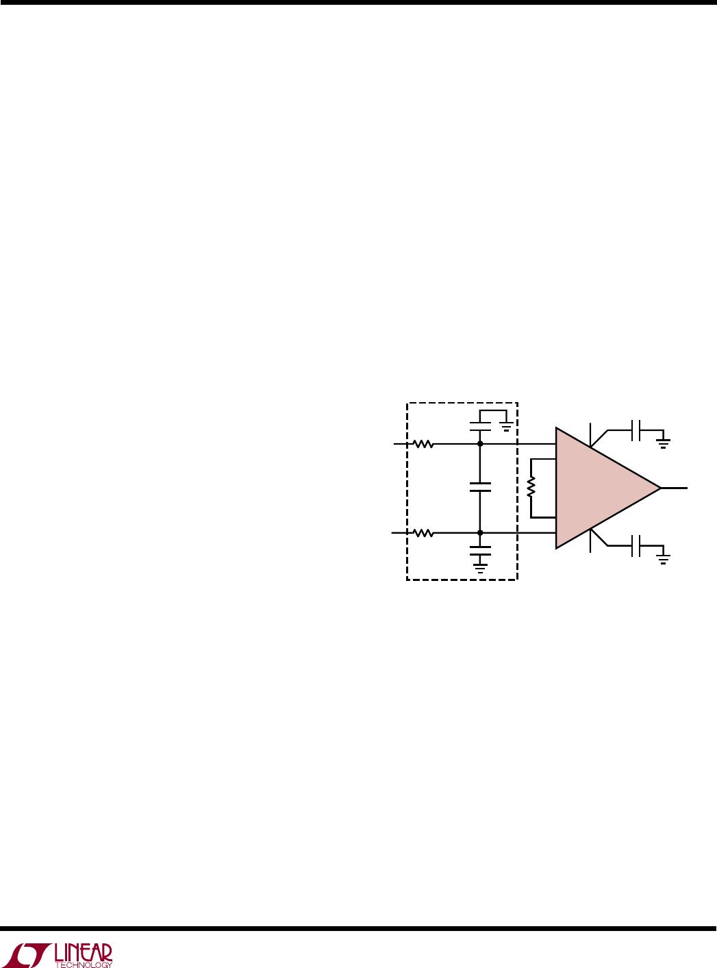
To significantly reduce the effect of these out-of-band
signals on the input offset voltage of instrumentation
amplifiers, simple lowpass filters can be used at the
inputs. This filter should be located very close to the input
pins of the circuit. An effective filter configuration is
illustrated in Figure 7, where three capacitors have been
added to the inputs of the LT1168. Capacitors C
XCM1
and
C
XCM2
form lowpass filters with the external series resis-
tors R
S1, 2
to any out-of-band signal appearing on each of
the input traces. Capacitor C
XD
forms a filter to reduce any
unwanted signal that would appear across the input traces.
An added benefit to using C
XD
is that the circuit’s AC
common mode rejection is not degraded due to common
mode capacitive imbalance. The differential mode and
common mode time constants associated with the capaci-
tors are:
t
DM(LPF)
= (R
S1
+ R
S2
)(C
XD
+ C
XCM1
+ C
XCM2
)
t
CM(LPF)
= (R
S1
||
R
S2
)(C
XCM1
+
C
XCM2
)
Setting the time constants requires a knowledge of the
frequency, or frequencies of the interference. Once this
frequency is known, the common mode time constants
can be set followed by the differential mode time constant.
To avoid any possibility of inadvertently affecting the
signal to be processed, set the common mode time
constant an order of magnitude (or more) smaller than the
differential mode time constant. Set the common mode
time constants such that they do not degrade the LT1168
inherent AC CMR. Then the differential mode time con-
stant can be set for the bandwidth required for the appli-
cation. Setting the differential mode time constant close to
the sensor’s BW also minimizes any noise pickup along
the leads. To avoid any possibility of common mode to
differential mode signal conversion, match the common
mode time constants to 1% or better. If the sensor is an
RTD or a resistive strain gauge and is in proximity to the
instrumentation amplifier, then the series resistors R
S1, 2
can be omitted.
Figure 7. Adding a Simple RC Filter at the Inputs to an
Instrumentation Amplifier is Effective in Reducing Rectification
of High Frequency Out-of-Band Signals
APPLICATIO S I FOR ATIO
WUUU
–V
S
+V
S
IN
+
IN
1168 F07
V
OUT
R
G
C
XCM1
0.001µF
C
XCM2
0.001µF
C
XD
0.1µF
R
S1
1.6k
R
S2
1.6k
EXTERNAL RFI
FILTER
+
LT1168
f
3dB
500Hz
Nerve Impulse Amplifier
The LT1168’s low current noise makes it ideal for EMG
monitors that have high source impedances. Demonstrat-
ing the LT1168’s ability to amplify low level signals, the
circuit in Figure 8 takes advantage of the amplifier’s high
gain and low noise operation. This circuit amplifies the low
level nerve impulse signals received from a patient at
Pins 2 and 3. R
G
and the parallel combination of R3 and R4
set a gain of ten. The potential on LT1112’s Pin 1 creates

LT1168ACN8#PBF

Mfr. #:
Manufacturer:
Analog Devices Inc.
Description:
Instrumentation Amplifiers L Pwr, 1x Res Gain Progmable, Prec Instr
Lifecycle:
New from this manufacturer.
Delivery:
DHL FedEx Ups TNT EMS
Payment:
T/T Paypal Visa MoneyGram Western Union