4
LT1168
1168fa
The denotes the specifications which apply over the 0°C T
A
70°C
temperature range. V
S
= ±15V, V
CM
= 0V, R
L
= 10k unless otherwise noted.
The
denotes the specifications which apply over the –40°C T
A
85°C temperature range. V
S
= ±15V, V
CM
= 0V, R
L
= 10k unless
otherwise noted. (Note 8)
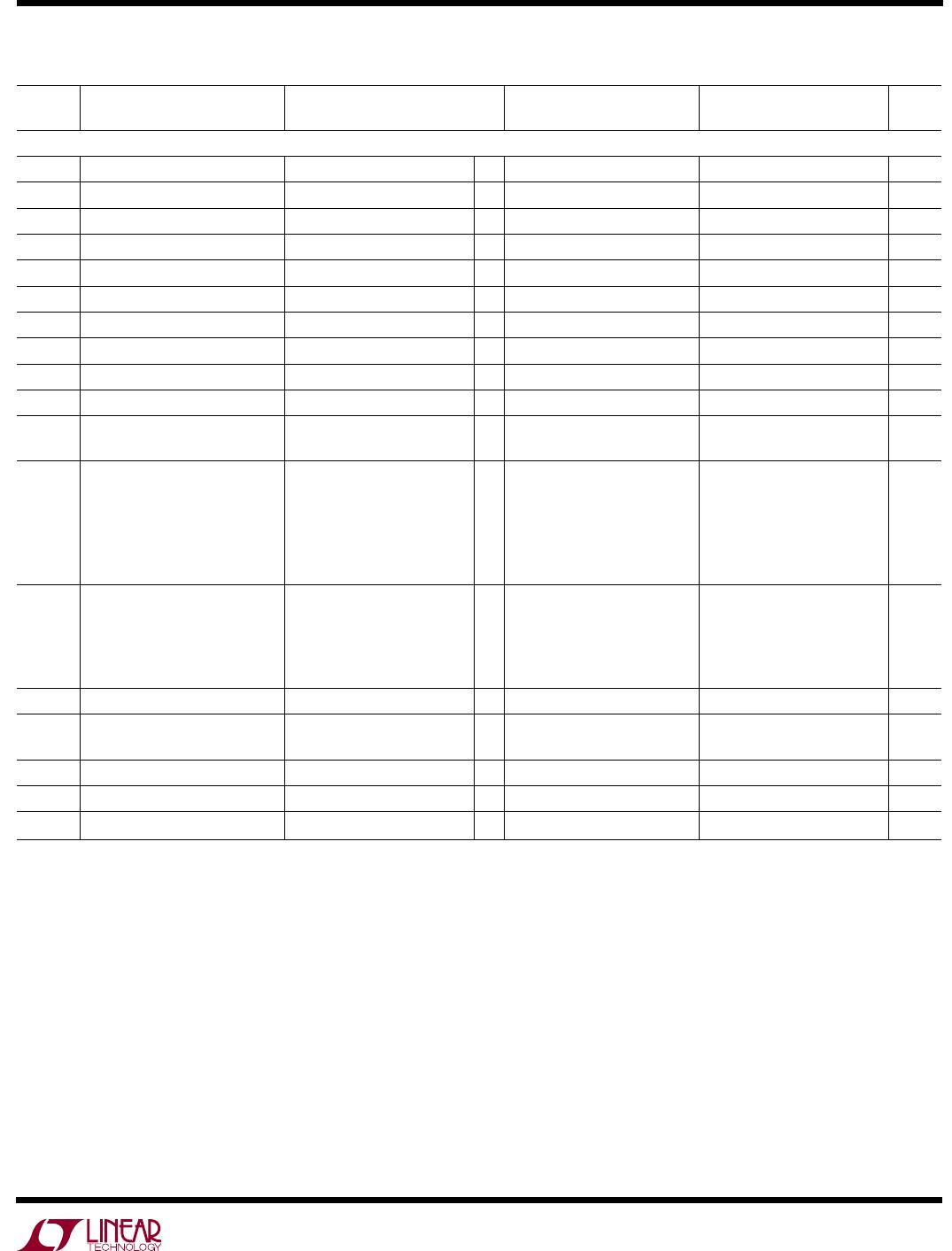
LT1168AI LT1168I
SYMBOL PARAMETER CONDITIONS (Note 6) MIN TYP MAX MIN TYP MAX UNITS
Gain Error G = 1 0.014 0.04 0.015 0.05 %
G = 10 (Note 7)
0.600 1.9 0.700 2.0 %
G = 100 (Note 7)
0.600 2.0 0.700 2.1 %
G = 1000 (Note 7)
0.600 2.1 0.700 2.2 %
G
N
Gain Nonlinearity V
O
= ±10V, G = 1 3 20 5 25 ppm
(Notes 7, 8) V
O
= ±10V, G = 10 and 100 10 35 15 40 ppm
VO = ±10V, G = 1000
30 70 35 100 ppm
G/T Gain vs Temperature G < 1000 (Note 7) 100 200 100 200 ppm/°C
LT1168AC LT1168C
SYMBOL PARAMETER CONDITIONS (Note 6) MIN TYP MAX MIN TYP MAX UNITS
V
OST
Total Input Referred Offset Voltage V
OST
= V
OSI
+ V
OSO
/G
V
OSI
Input Offset Voltage V
S
= ±5V to ±15V 18 60 23 80 µV
V
OSIH
Input Offset Voltage Hysteresis (Notes 7, 10) 3.0 3.0 µV
V
OSO
Output Offset Voltage V
S
= ±5V to ±15V 60 380 70 500 µV
V
OSOH
Output Offset Voltage Hysteresis (Notes 7, 10) 30 30 µV
V
OSI
/T Input Offset Drift (RTI) (Note 9) 0.05 0.3 0.06 0.4 µV/°C
V
OSO
/T Output Offset Drift (Note 9) 0.7 3 0.8 4 µV/°C
I
OS
Input Offset Current 100 400 120 550 pA
I
OS
/T Input Offset Current Drift 0.3 0.4 pA/°C
I
B
Input Bias Current 65 350 105 600 pA
I
B
/T Input Bias Current Drift 1.4 1.4 pA/°C
V
CM
Input Voltage Range G = 1, Other Input Grounded
V
S
= ±2.3V to ±5V –V
S
+ 2.1 +V
S
– 1.3 –V
S
+ 2.1 +V
S
– 1.3 V
V
S
= ±5V to ±18V –V
S
+ 2.1 +V
S
– 1.4 –V
S
+ 2.1 +V
S
– 1.4 V
CMRR Common Mode 1k Source Imbalance,
Rejection Ratio V
CM
= 0V to ±10V
G = 1
88 92 83 92 dB
G = 10
100 110 97 110 dB
G = 100
115 120 113 120 dB
G = 1000
117 135 114 135 dB
PSRR Power Supply V
S
= ±2.3V to ±18V
Rejection Ratio G = 1
102 115 98 115 dB
G = 10
123 130 118 130 dB
G = 100
127 135 124 135 dB
G = 1000
129 145 126 145 dB
I
S
Supply Current V
S
= ±2.3V to ±18V 390 615 390 615 µA
V
OUT
Output Voltage Swing R
L
= 10k
V
S
= ±2.3V to ±5V –V
S
+ 1.4 +V
S
– 1.3 –V
S
+ 1.4 +V
S
– 1.3 V
V
S
= ±5V to ±18V –V
S
+ 1.6 +V
S
– 1.5 –V
S
+ 1.6 +V
S
– 1.5 V
I
OUT
Output Current 16 25 16 25 mA
SR Slew Rate G = 1, V
OUT
= ±10V 0.25 0.48 0.25 0.48 V/µs
V
REF
Voltage Range (Note 9) –V
S
+ 1.6 +V
S
– 1.6 –V
S
+ 1.6 +V
S
– 1.6 V
ELECTRICAL CHARACTERISTICS
5
LT1168
1168fa
Note 1: Stresses beyond those listed under Absolute Maximum Ratings
may cause permanent damage to the device. Exposure to any Absolute
Maximum Rating condition for extended periods may affect device
reliability and lifetime.
Note 2: If the input voltage exceeds the supplies, the input current should
be limited to less than 20mA.
Note 3: A heat sink may be required to keep the junction temperature
below absolute maximum.
Note 4: The LT1168AC/LT1168C are guaranteed functional over the
operating temperature range of –40°C and 85°C.
Note 5: The LT1168AC/LT1168C are guaranteed to meet specified
performance from 0°C to 70°C. The LT1168AC/LT1168C are designed,
characterized and expected to meet specified performance from –40°C
to 85°C but are not tested or QA sampled at these temperatures. The
LT1168AI/LT1168I are guaranteed to meet specified performance from
–40°C to 85°C.
Note 6: Typical parameters are defined as the 60% of the yield parameter
distribution.
Note 7: Does not include the tolerance of the external gain resistor R
G
.
Note 8: This parameter is measured in a high speed automatic tester that
does not measure the thermal effects with longer time constants. The
magnitude of these thermal effects are dependent on the package used,
heat sinking and air flow conditions.
Note 9: This parameter is not 100% tested.
Note 10: Hysteresis in offset voltage is created by package stress that
differs depending on whether the IC was previously at a higher or lower
temperature. Offset voltage hysteresis is always measured at 25°C, but
the IC is cycled to 85°C I-grade (or 70°C C-grade) or –40°C I-grade
(0°C C-grade) before successive measurement. 60% of the parts will
pass the typical limit on the data sheet.
The denotes the specifications which apply over the –40°C T
A
85°C
temperature range. V
S
= ±15V, V
CM
= 0V, R
L
= 10k unless otherwise noted. (Note 5)
ELECTRICAL CHARACTERISTICS
LT1168AI LT1168I
SYMBOL PARAMETER CONDITIONS (Note 6) MIN TYP MAX MIN TYP MAX UNITS
V
OST
Total Input Referred Offset Voltage V
OST
= V
OSI
+ V
OSO
/G
V
OSI
Input Offset Voltage 20 75 25 100 µV
V
OSIH
Input Offset Voltage Hysteresis (Notes 7, 10) 3.0 3.0 µV
V
OSO
Output Offset Voltage 180 500 200 600 µV
V
OSOH
Output Offset Voltage Hysteresis (Notes 7, 10) 30 30 µV
V
OSI
/T Input Offset Drift (RTI) (Note 9) 0.05 0.3 0.06 0.4 µV/°C
V
OSO
/T Output Offset Drift (Note 9) 0.8 5 1 6 µV/°C
I
OS
Input Offset Current 110 550 120 700 pA
I
OS
/T Input Offset Current Drift 0.3 0.3 pA/°C
I
B
Input Bias Current 120 500 220 800 pA
I
B
/T Input Bias Current Drift 1.4 1.4 pA/°C
V
CM
Input Voltage Range V
S
= ±2.3V to ±5V –V
S
+ 2.1 +V
S
– 1.3 –V
S
+ 2.1 +V
S
– 1.3 V
V
S
= ±5V to ±18V –V
S
+ 2.1 +V
S
– 1.4 –V
S
+ 2.1 +V
S
– 1.4 V
CMRR Common Mode 1k Source Imbalance,
Rejection Ratio V
CM
= 0V to ±10V
G = 1
86 90 81 90 dB
G = 10
98 105 95 105 dB
G = 100
114 118 112 118 dB
G = 1000
116 133 112 133 dB
PSRR Power Supply V
S
= ±2.3V to ±18V
Rejection Ratio G = 1
100 112 95 112 dB
G = 10
120 125 115 125 dB
G = 100
125 132 120 132 dB
G = 1000
128 140 125 140 dB
I
S
Supply Current 420 650 420 650 µA
V
OUT
Output Voltage Swing V
S
= ±2.3V to ±5V –V
S
+ 1.4 +V
S
– 1.3 –V
S
+ 1.4 +V
S
– 1.3 V
V
S
= ±5V to ±18V –V
S
+ 1.6 +V
S
– 1.5 –V
S
+ 1.6 +V
S
– 1.5 V
I
OUT
Output Current 15 22 15 22 mA
SR Slew Rate 0.22 0.41 0.22 0.42 V/µs
V
REF
Voltage Range (Note 9) –V
S
+ 1.6 +V
S
– 1.6 –V
S
+ 1.6 +V
S
– 1.6 V
6
LT1168
1168fa
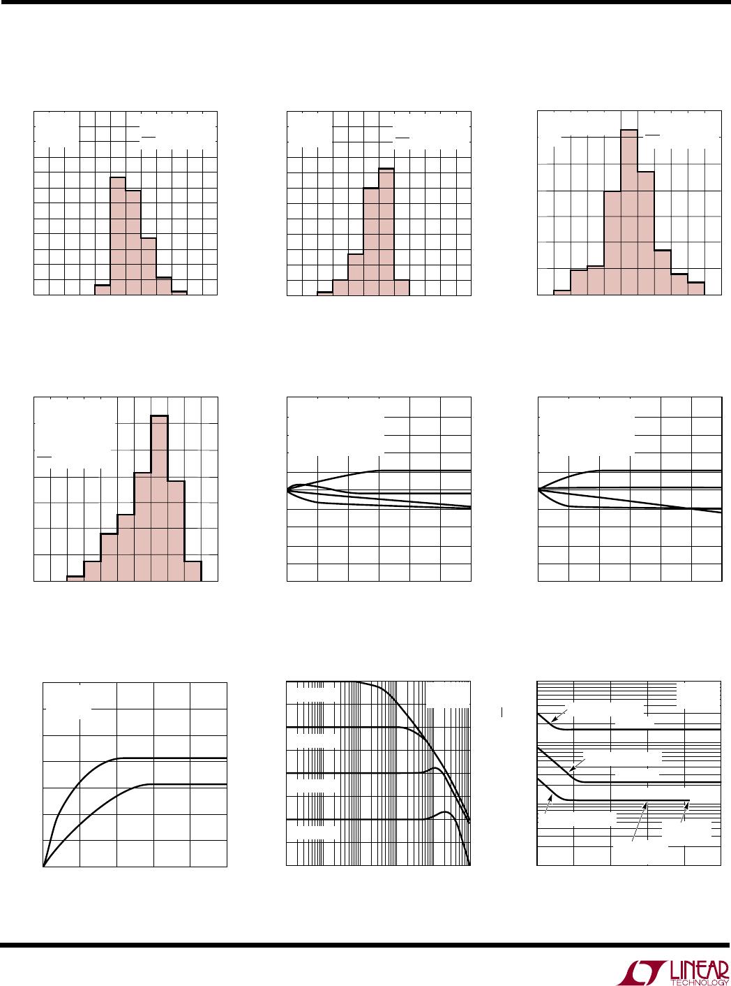
Distribution of Input Offset
Voltage
Distribution of Output Offset
Voltage
Distribution of Output Offset
Voltage Drift
Distribution of Input Offset
Voltage Drift
Output Offset Voltage
Long-Term Drift
TYPICAL PERFOR A CE CHARACTERISTICS
UW
OUTPUT OFFSET VOLTAGE (µV)
150
0
PERCENT OF UNITS (%)
10
20
30
40
60
100
–50 0 50
1168 G01
100 150
50
5
15
25
35
55
45
V
S
= ±15V
T
A
= 25°C
G = 1
299 N8 (2 LOTS)
337 S0-8 (2 LOTS)
636 TOTAL PARTS
INPUT OFFSET VOLTAGE (µV)
–60
0
PERCENT OF UNITS (%)
10
20
30
40
60
–40
–20 0 20
1168 G02
40 60
50
5
15
25
35
55
45
V
S
= ±15V
T
A
= 25°C
G = 1000
299 N8 (2 LOTS)
337 S0-8 (2 LOTS)
636 TOTAL PARTS
OUTPUT OFFSET VOLTAGE DRIFT (µV/°C)
1.8
0
PERCENT OF UNITS (%)
5
15
20
25
35
1168 G03
10
30
1.0
0.2
1.4
0.6 0.2
V
S
= ±15V
T
A
= –40°C TO 85°C
G = 1
97 N8 (2 LOTS)
49 S0-8 (1 LOT)
146 TOTAL PARTS
INPUT OFFSET VOLTAGE DRIFT (µV/°C)
0.45
0
PERCENT OF UNITS (%)
5
15
20
25
35
1168 G04
10
30
0.25
0.05
0.35
0.15 0.05
97 N8 (2 LOTS)
49 S0-8 (1 LOT)
146 TOTAL PARTS
V
S
= ±15V
T
A
= –40°C TO 85°C
G = 1000
TIME (MONTHS)
0
–50
CHANGE IN OUTPUT OFFSET VOLTAGE (µV)
–30
–10
10
1
2
1168 G05
30
50
–40
–20
0
20
40
3
V
S
= ±15V
T
A
= 30°C
G = 1
4 PARTS FROM 4 LOTS
WARMED UP
Input Offset Voltage
Long-Term Drift
TIME (MONTHS)
0
–5
CHANGE IN INPUT OFFSET VOLTAGE (µV)
–3
–1
1
1
2
1168 G05
3
5
–4
–2
0
2
4
3
V
S
= ±15V
T
A
= 30°C
G = 1000
4 PARTS FROM 4 LOTS
WARMED UP
Warm-Up Drift Gain vs Frequency
Voltage Noise Density
vs Frequency
TIME AFTER POWER-ON (MINUTES)
012345
CHANGE IN TOTAL INPUT REFERRED
OFFSET VOLTAGE (µV)
1168 G07
35
30
25
20
15
10
5
0
SO-8
N-8
V
S
= ±15V
T
A
= 25°C
G = 1
FREQUENCY (kHz)
GAIN (dB)
1168 G08
0.01
60
50
40
30
20
10
0
–10
–20
1 100 10000.1 10
G = 1000
G = 100
G = 10
G = 1
V
S
= ±15V
T
A
= 25°C
FREQUENCY (Hz)
1 10 100 1k 10k 100k
1
VOLTAGE NOISE DENSITY (nV/Hz)
10
100
1000
1168 G09
V
S
= ±15V
T
A
= 25°C
1/f CORNER = 2Hz
GAIN = 1
GAIN = 10
GAIN = 100, 1000
1/f CORNER = 7Hz
1/f CORNER = 3Hz
BW LIMIT
GAIN = 1000
BW LIMIT
GAIN = 100

LT1168ACN8#PBF

Mfr. #:
Manufacturer:
Analog Devices Inc.
Description:
Instrumentation Amplifiers L Pwr, 1x Res Gain Progmable, Prec Instr
Lifecycle:
New from this manufacturer.
Delivery:
DHL FedEx Ups TNT EMS
Payment:
T/T Paypal Visa MoneyGram Western Union