MAX1011
Low-Power, 90Msps, 6-Bit ADC
4 _______________________________________________________________________________________
__________________________________________Typical Operating Characteristics
(V
CC
= +5V ±5%, V
CCO
= 3.3V ±300mV, f
CLK
= 90Msps, GAIN = open (midgain) MAX1011 evaluation kit, T
A
= +25°C, unless
otherwise noted.)
6.0
5.0
10
100
EFFECTIVE NUMBER OF BITS
vs. ANALOG INPUT FREQUENCY
5.2
MAX1011-01
ANALOG INPUT FREQUENCY (MHz)
EFFECTIVE NUMBER OF BITS
5.4
5.6
5.8
f
CLK
= 90Msps
-1.0
1 10 100
ANALOG INPUT BANDWIDTH
-0.8
MAX1011-02
ANALOG INPUT FREQUENCY (MHz)
MAGNITUDE (dB)
-0.6
-0.2
-0.4
0
5.5
1 10 100
EFFECTIVE NUMBER OF BITS
vs. SAMPLING/CLOCK FREQUENCY
5.6
MAX1011-03
CLOCK FREQUENCY (MHz)
EFFECTIVE NUMBER OF BITS
5.7
5.9
5.8
6.0
f
IN
= 20MHz
-50
1k 100k 1M
OSCILLATOR OPEN-LOOP PHASE NOISE
vs. FREQUENCY OFFSET
-110
-130
-90
-70
MAX1011-04
FREQUENCY OFFSET FROM CARRIER (Hz)
PHASE NOISE (dBc)
10k
0.50
-0.50
0 64
DIFFERENTIAL NONLINEARITY
vs. CODE
-0.25
0.25
MAX1003-07
CODE
DNL (LSB)
10 20 30 40 50 60
0
_______________Detailed Description
Converter Operation
The MAX1011 integrates a 6-bit analog-to-digital con-
verter (ADC), a buffered voltage reference, and oscilla-
tor circuitry. The ADC uses a flash conversion technique
to convert an analog input signal into a 6-bit parallel
digital output code. The MAX1011’s unique design
includes 63 fully differential comparators and a propri-
etary encoding scheme that ensures no more than
1LSB dynamic encoding error. The control logic inter-
faces easily to most digital signal processors (DSPs)
and microprocessors (µPs) with +3.3V CMOS-compati-
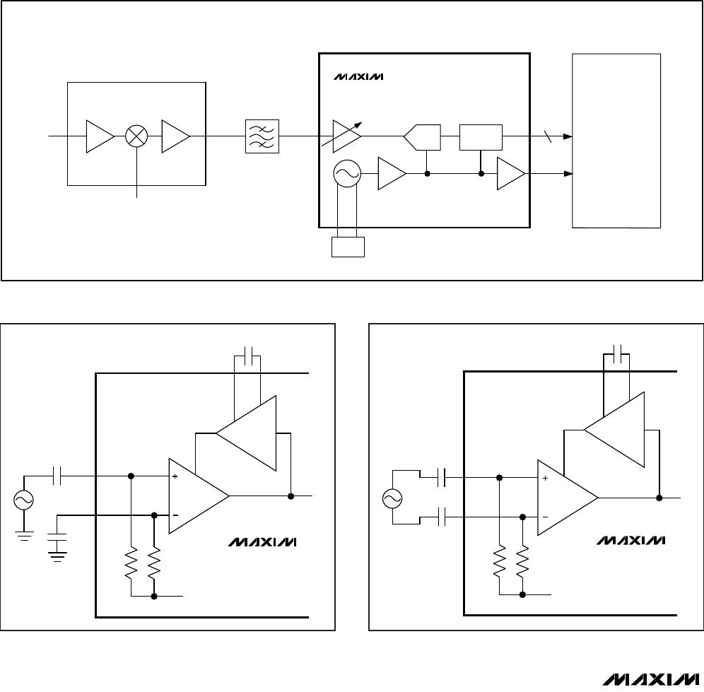
ble logic interfaces. Figure 1 shows the MAX1011 in a
typical application.
Programmable Input Amplifier
The MAX1011 has a programmable-gain input amplifier
with a -0.5dB bandwidth of 55MHz and a true differen-
tial input. To maximize performance in high-speed
systems, the amplifier has less than 3pF of input
capacitance. The input amplifier gain is programmed
via the GAIN pin to provide three possible input full-
scale ranges (FSRs) as shown in Table 1.
Single-ended and differential AC-coupled input circuit
examples are shown in Figures 2 and 3. Each of the
MAX1011
Low-Power, 90Msps, 6-Bit ADC
_______________________________________________________________________________________ 5
Pin Description
PIN
Gain-Select Input. Sets input full-scale range: 125/250/500mVp-p (Table 1).GAIN1
FUNCTIONNAME
Positive Offset-Correction Compensation. Connect a 0.22µF capacitor for AC-coupled inputs. Ground
pin 2 for DC-coupled inputs.
OCC+2
Noninverting Analog InputIN+4
Negative Offset-Correction Compensation. Connect a 0.22µF capacitor for AC-coupled inputs. Ground
pin 3 for DC-coupled inputs.
OCC-3
+5V ±5% Supply. Bypass with a 0.01µF capacitor to GND (pin 9).V
CC
6
Analog GroundGND
9, 10,
12, 13
Inverting Analog InputIN-5
+5V ±5% Supply. Bypass with a 0.01µF capacitor to GND (pin 10).V
CC
11
Digital Clock Output. Frames the output data.DCLK18
Digital Output Supply, +3.3V ±300mV. Bypass with a 47pF capacitor to OGND (pin 16).V
CCO
17
Digital Outputs 0–5. D5 is the most significant bit (MSB).D0–D519–24
250Open
125V
CC
GAIN
500GND
INPUT FULL-SCALE RANGE
(mVp-p)
Table 1. Input Amplifier Programming
Positive Oscillator/Clock InputTNK+7
Negative Oscillator/Clock InputTNK-8
No ConnectionN.C.15
Digital Output GroundOGND16
+5V ±5% Supply. Bypass with a 0.01µF capacitor to GND (pin 13).V
CC
14
MAX1011
amplifier inputs is internally biased to a 2.35V reference
through a 20k resistor, eliminating external DC bias
circuits. A series 0.1µF capacitor is required at the
amplifier input for AC-coupled signals.
When operating with AC-coupled inputs, the input
amplifier’s DC offset voltage is nulled to within ±1/2LSB
by an on-chip, offset-correction amplifier. An external
compensation capacitor is required to set the dominant
pole of the offset-correction amplifier’s frequency
response (Figures 2 and 3). The compensation capaci-
tor will determine the low-frequency corner of the ana-
log input response according to the following formula:
f
c
= 1 / (0.1 x C)
where C is the value of the compensation capacitor in
µF, and f
c
is the corner frequency in Hz.
Low-Power, 90Msps, 6-Bit ADC
6 _______________________________________________________________________________________
6 BITS
DATA
BUFFER
DIGITAL
DEMODULATOR
OR
DSP
6
DCLK
TANK
MAX1011
LO
RF
Figure 1. IF Sampling Receiver
Figure 2. Single-Ended AC-Coupled Input
Figure 3. Differential AC-Coupled Input
MAX1011
INPUT
AMP
20k
2.35V INTERNAL REFERENCE
20k
IN+
OCC+ OCC-
IN-
0.1µF
0.22µF
V
SOURCE
0.1µF
OFFSET
CORREC-
TION
MAX1011
INPUT
AMP
20k
2.35V INTERNAL REFERENCE
20k
IN+
OCC+ OCC-
IN-
0.1µF
0.1µF
V
SOURCE
OFFSET
CORREC-
TION
0.22µF

MAX1011CEG+

Mfr. #:
Manufacturer:
Maxim Integrated
Description:
Analog to Digital Converters - ADC Low-Power 90Msps 6-Bit
Lifecycle:
New from this manufacturer.
Delivery:
DHL FedEx Ups TNT EMS
Payment:
T/T Paypal Visa MoneyGram Western Union

Products related to this Datasheet