© Semiconductor Components Industries, LLC, 2017
January, 2017 − Rev. 18
1 Publication Order Number:
NCS2001/D
NCS2001, NCV2001
0.9 V, Rail-to-Rail, Single
Operational Amplifier
The NCS2001 is an industry first sub−one voltage operational
amplifier that features a rail−to−rail common mode input voltage range,
along with rail−to−rail output drive capability. This amplifier is
guaranteed to be fully operational down to 0.9 V, providing an ideal
solution for powering applications from a single cell Nickel Cadmium
(NiCd) or Nickel Metal Hydride (NiMH) battery. Additional features
include no output phase reversal with overdriven inputs, trimmed input
offset voltage of 0.5 mV, extremely low input bias current of 40 pA, and
a unity gain bandwidth of 1.4 MHz at 5.0 V. The tiny NCS2001 is the
ideal solution for small portable electronic applications and is available
in the space saving SOT23−5 and SC70−5 packages with two industry
standard pinouts.
Features
0.9 V Guaranteed Operation
Rail−to−Rail Common Mode Input Voltage Range
Rail−to−Rail Output Drive Capability
No Output Phase Reversal for Over−Driven Input Signals
0.5 mV Trimmed Input Offset
10 pA Input Bias Current
1.4 MHz Unity Gain Bandwidth at "2.5 V, 1.1 MHz at "0.5 V
Tiny SC70−5 and SOT23−5 Packages
NCV Prefix for Automotive and Other Applications Requiring
Unique Site and Control Change Requirements; AEC−Q100
Qualified and PPAP Capable
These Devices are Pb−Free, Halogen Free/BFR Free and are RoHS
Compliant
Typical Applications
Single Cell NiCd/NiMH Battery Powered Applications
Cellular Telephones
Pagers
Personal Digital Assistants
Electronic Games
Digital Cameras
Camcorders
Hand−Held Instruments
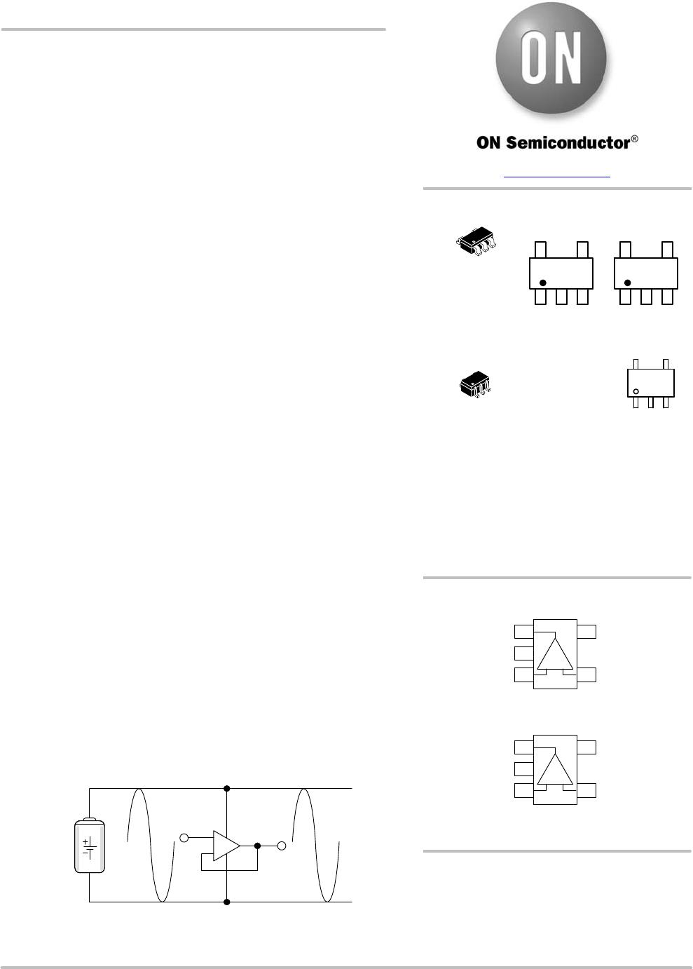
Figure 1. Typical Application
This device contains 63 active transistors.
-
+
0.8 V
to
7.0 V
Rail to Rail Input Rail to Rail Output
www.onsemi.com
ORDERING INFORMATION
SOT23−5
SN SUFFIX
CASE 483
PIN CONNECTIONS
1
V
OUT
V
CC
Non−Inverting
Input
2
3
5
4
V
EE
Inverting
Input
Style 1 Pinout (SN1T1, SQ1T2)
+−
1
V
OUT
V
EE
Non−Inverting
Input
2
3
5
4
V
CC
Inverting
Input
Style 2 Pinout (SN2T1, SQ2T2)
+−
MARKING DIAGRAMS
x = G for SN1
H for SN2
I for SQ1
J for SQ2
A = Assembly Location
Y = Year
W = Work Week
M = Date Code
G = Pb−Free Package
1
2
3
4
5
SC70−5
SQ SUFFIX
CASE 419A
M
1
5
See detailed ordering and shipping information in the
p
dimensions section on page 14 of this data sheet.
AAx
|
(Note: Microdot may be in either location)
1
5
MBB AYWG
G
1
5
AAx AYWG
G
NCV2001SN2
1
5
NCS2001, NCV2001
www.onsemi.com
2
MAXIMUM RATINGS
Rating Symbol Value Unit
Supply Voltage (V
CC
to V
EE
) V
S
7.0 V
Input Differential Voltage Range (Note 1) V
IDR
V
EE
−300 mV to 7.0 V V
Input Common Mode Voltage Range (Note 1) V
ICR
V
EE
−300 mV to 7.0 V V
Output Short Circuit Duration (Note 2) t
Sc
Indefinite sec
Junction Temperature T
J
150 °C
Power Dissipation and Thermal Characteristics
SOT23−5 Package
Thermal Resistance, Junction−to−Air
Power Dissipation @ T
A
= 70°C
SC70−5 Package
Thermal Resistance, Junction−to−Air
Power Dissipation @ T
A
= 70°C
R
q
JA
P
D
R
q
JA
P
D
235
340
280
286
°C/W
mW
°C/W
mW
Operating Ambient Temperature Range
NCS2001
NCV2001 (Note 3)
T
A
−40 to +105
−40 to +125
°C
Storage Temperature Range T
stg
−65 to 150 °C
ESD Protection at any Pin Human Body Model (Note 4) V
ESD
1500 V
Stresses exceeding those listed in the Maximum Ratings table may damage the device. If any of these limits are exceeded, device functionality
should not be assumed, damage may occur and reliability may be affected.
1. Either or both inputs should not exceed the range of V
EE
−300 mV to V
EE
+7.0 V.
2. Maximum package power dissipation limits must be observed to ensure that the maximum junction temperature is not exceeded.
T
J
= T
A
+ (P
D
R
q
JA
).
3. NCV prefix is qualified for automotive usage.
4. ESD data available upon request.
DC ELECTRICAL CHARACTERISTICS
(V
CC
= 2.5 V, V
EE
= −2.5 V, V
CM
= V
O
= 0 V, R
L
to GND, T
A
= 25°C unless otherwise noted.)
Characteristics
Symbol Min Typ Max Unit
Input Offset Voltage
V
CC
= 0.45 V, V
EE
= −0.45 V
T
A
= 25°C
T
A
= 0°C to 70°C
T
A
= −40°C to 125°C
V
CC
= 1.5 V, V
EE
= −1.5 V
T
A
= 25°C
T
A
= 0°C to 70°C
T
A
= −40°C to 125°C
V
CC
= 2.5 V, V
EE
= −2.5 V
T
A
= 25°C
T
A
= 0°C to 70°C
T
A
= −40°C to 125°C
V
IO
−6.0
−8.5
−9.5
−6.0
−7.0
−7.5
−6.0
−7.5
−7.5
0.5
0.5
0.5
6.0
8.5
9.5
6.0
7.0
7.5
6.0
7.5
7.5
mV
Input Offset Voltage Temperature Coefficient (R
S
= 50)
T
A
= −40°C to 125°C
DV
IO
/DT
8.0
mV/°C
Input Bias Current (V
CC
= 1.0 V to 5.0 V) I
IB
10 pA
Input Common Mode Voltage Range V
ICR
V
EE
to V
CC
V
Large Signal Voltage Gain
V
CC
= 0.45 V, V
EE
= −0.45 V
R
L
= 10 k
R
L
= 2.0 k
V
CC
= 1.5 V, V
EE
= −1.5 V
R
L
= 10 k
R
L
= 2.0 k
V
CC
= 2.5 V, V
EE
= −2.5 V
R
L
= 10 k
R
L
= 2.0 k
A
VOL
20
15
40
20
40
40
40
40
kV/V
NCS2001, NCV2001
www.onsemi.com
3
DC ELECTRICAL CHARACTERISTICS (continued)
(V
CC
= 2.5 V, V
EE
= −2.5 V, V
CM
= V
O
= 0 V, R
L
to GND, T
A
= 25°C unless otherwise noted.)
Characteristics UnitMaxTypMinSymbol
Output Voltage Swing, High State Output (V
ID
= +0.5 V)
V
CC
= 0.45 V, V
EE
= −0.45 V
T
A
= 25°C
R
L
= 10 k
R
L
= 2.0 k
T
A
= 0°C to 70°C
R
L
= 10 k
R
L
= 2.0 k
T
A
= −40°C to 125°C
R
L
= 10 k
R
L
= 2.0 k
V
CC
= 1.5 V, V
EE
= −1.5 V
T
A
= 25°C
R
L
= 10 k
R
L
= 2.0 k
T
A
= 0°C to 70°C
R
L
= 10 k
R
L
= 2.0 k
T
A
= −40°C to 125°C
R
L
= 10 k
R
L
= 2.0 k
V
CC
= 2.5 V, V
EE
= −2.5 V
T
A
= 25°C
R
L
= 10 k
R
L
= 2.0 k
T
A
= 0°C to 70°C
R
L
= 10 k
R
L
= 2.0 k
T
A
= −40°C to 125°C
R
L
= 10 k
R
L
= 2.0 k
V
OH
0.40
0.35
0.40
0.35
0.40
0.35
1.45
1.40
1.45
1.40
1.45
1.40
2.45
2.40
2.45
2.40
2.45
2.40
0.494
0.466
1.498
1.480
2.498
2.475
V
Output Voltage Swing, Low State Output (V
ID
= −0.5 V)
V
CC
= 0.45 V, V
EE
= −0.45 V
T
A
= 25°C
R
L
= 10 k
R
L
= 2.0 k
T
A
= 0°C to 70°C
R
L
= 10 k
R
L
= 2.0 k
T
A
= −40°C to 125°C
R
L
= 10 k
R
L
= 2.0 k
V
CC
= 1.5 V, V
EE
= −1.5 V
T
A
= 25°C
R
L
= 10 k
R
L
= 2.0 k
T
A
= 0°C to 70°C
R
L
= 10 k
R
L
= 2.0 k
T
A
= −40°C to 125°C
R
L
= 10 k
R
L
= 2.0 k
V
CC
= 2.5 V, V
EE
= −2.5 V
T
A
= 25°C
R
L
= 10 k
R
L
= 2.0 k
T
A
= 0°C to 70°C
R
L
= 10 k
R
L
= 2.0 k
T
A
= −40°C to 125°C
R
L
= 10 k
R
L
= 2.0 k
V
OL
−0.494
−0.480
−1.493
−1.480
−2.492
−2.479
−0.40
−0.35
−0.40
−0.35
−0.40
−0.35
−1.45
−1.40
−1.45
−1.40
−1.45
−1.40
−2.45
−2.40
−2.45
−2.40
−2.45
−2.40
V

NCS2001SQ2T2G

Mfr. #:
Manufacturer:
ON Semiconductor
Description:
Operational Amplifiers - Op Amps 0.9V Single Rail to Rail -40 to 105 Cel
Lifecycle:
New from this manufacturer.
Delivery:
DHL FedEx Ups TNT EMS
Payment:
T/T Paypal Visa MoneyGram Western Union