NCS2001, NCV2001
www.onsemi.com
7
T
A
, Ambient Temperature (°C)
2.0
−50 −25 0 25 50 75 100
1.5
1.0
0.5
0
125
R
L
= 10 k
C
L
= 10 pF
T
A
= 25°C
+Slew Rate, V
S
= ±0.45 V
−Slew Rate, V
S
= ±2.5 V
−Slew Rate, V
S
= ±0.45 V
+Slew Rate, V
S
= ±2.5 V
SR, Slew Rate (V/
m
s)
2.5
10
1.0
0.1
0.01
−50 −25 0 25 50 75 100 12
5
T
A
, Ambient Temperature (°C)
V
CC
= 2.5 V
V
EE
= −2.5 V
R
L
= 10 k
C
L
= 10 pF
10
1.0
0.01
0.1
f, Frequency (Hz)
10 1.0 k100 100 k10 k
V
S
= ±2.5 V
V
out
= 4.0 V
pp
R
L
= 2.0 k
T
A
= 25°C
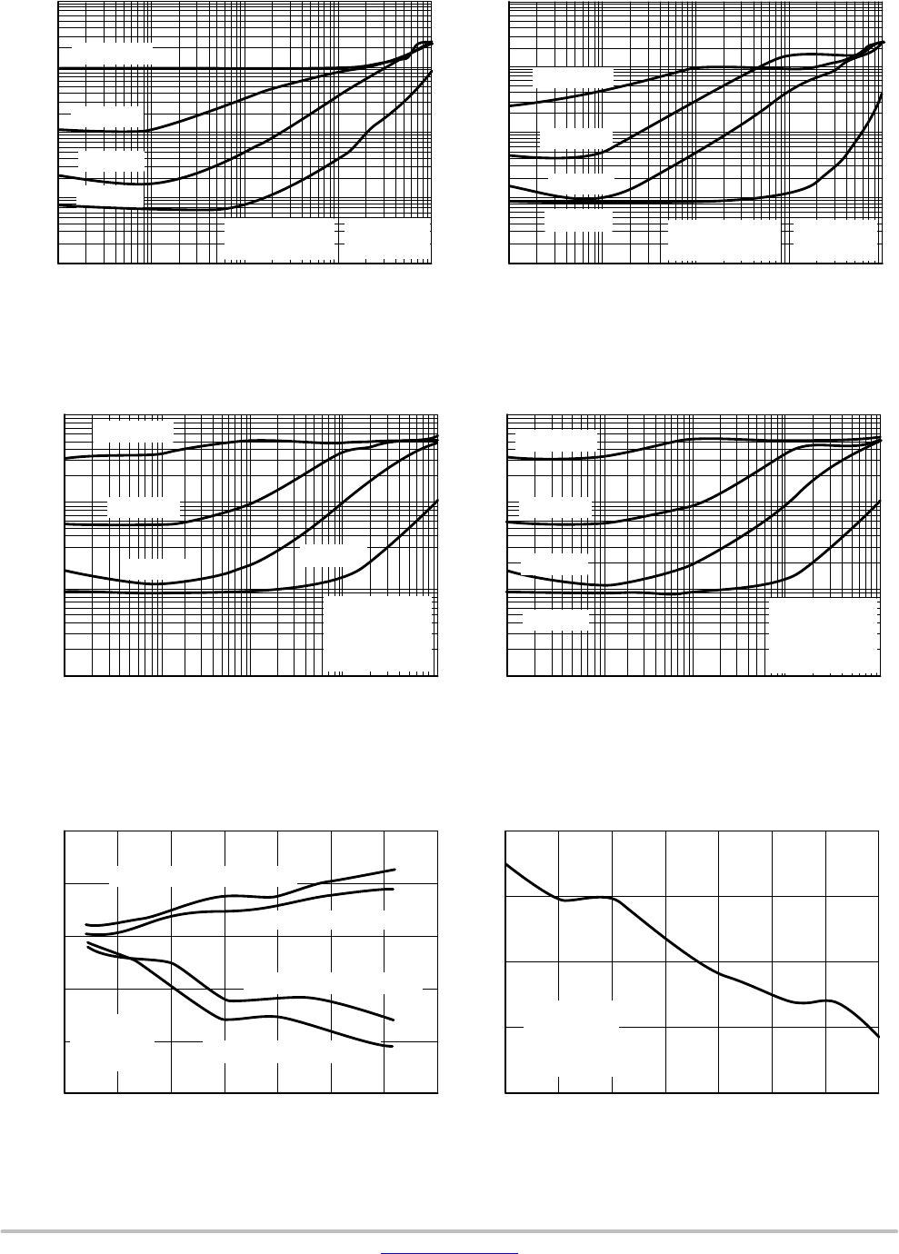
Figure 14. Total Harmonic Distortion vs.
Frequency with 1.0 V Supply
Figure 15. Total Harmonic Distortion vs.
Frequency with 1.0 V Supply
Figure 16. Total Harmonic Distortion vs.
Frequency with 5.0 V Supply
Figure 17. Total Harmonic Distortion vs.
Frequency with 5.0 V Supply
f, Frequency (Hz)
f, Frequency (Hz)
f, Frequency (Hz)
10
10
1.0
1.0 k100
0.1
0.001
10 k 100 k
R
L
= 2.0 k
T
A
= 25°C
A
V
= 1.0
A
V
= 10
A
V
= 100
A
V
= 1000
10 1.0 k 10 k100 100
k
0.01
0.1
1.0
10
10 1.0 k100 100 k10 k
V
S
= ±2.5 V
V
out
= 4.0 V
pp
R
L
= 10 k
T
A
= 25°C
Figure 18. Slew Rate vs. Temperature Figure 19. Gain Bandwidth Product vs.
Temperature
THD, Total Harmonic Distortion (%)
GBW, Gain Bandwidth Product (MHz)
V
S
= ±0.5 V
V
out
= 0.4 V
pp
R
L
= 10 k
T
A
= 25°C
V
S
= ±0.5 V
V
out
= 0.4 V
pp
A
V
= 1.0
A
V
= 10
A
V
= 100
A
V
= 1000
A
V
= 1.0
A
V
= 10
A
V
= 100
A
V
= 1000
0.01
A
V
= 1.0
A
V
= 10
A
V
= 100
A
V
= 1000
0.001
0.9
1.0
1.1
1.2
1.3
NCS2001, NCV2001
www.onsemi.com
8
0 0.5 1.0 1.5 2.0 2.5 3.0 3.5
80
0
60
40
20
V
S
, Supply Voltage (V)
Phase Margin
100
0
60
40
20
Gain Margin
R
L
= 10 k
C
L
= 10 pF
T
A
= 25°C
Fm, Phase Margin (°)
A
m
, Gain Margin (dB)
100
80
Phase Margin
Gain Margin
80
0
60
40
20
C
L
, Output Load Capacitance (pF)
A
V
= 100
V
CC
= 2.5 V
V
EE
= −2.5 V
R
L
= 10 k to GND
T
A
= 25°C
80
0
60
40
20
1.0 100 100010
Am, Gain Margin (dB)
Fm, Phase Margin (°)
100
100
100
0
60
40
20
80
0
60
40
20
Phase Margin
Gain Margin
−50 −25 0 25 50 75 100 125
V
CC
= 2.5 V
V
EE
= −2.5 V
R
L
= 10 k
C
L
= 10 pF
T
A
, Ambient Temperature (°C)
Am, Gain Margin (dB)
Fm, Phase Margin (°)
80
100
V
S
= ±0.5 V
−20
0
20
40
60
80
−180
−135
−90
−45
R
L
= 10 k
T
A
= 25°C
10 k 100 k 1.0 M 10 M 100 M
−225
V
S
= ±2.5 V
−40
Fm, Phase Margin (°)
10 100 1.0 k 100 k
Phase Margin
Gain Margin
10 k
0
10
20
30
40
60
50
70
V
CC
= 2.5 V
V
EE
= −2.5 V
R
L
= 10 k
C
L
= 10 pF
T
A
= 25°C
0
10
20
30
40
60
50
70
R
t
, Differential Source Resistance (W)
Figure 20. Voltage Gain and Phase vs.
Frequency
Figure 21. Gain and Phase Margin vs.
Temperature
Figure 22. Gain and Phase Margin vs.
Differential Source Resistance
Figure 23. Gain and Phase Margin vs.
Output Load Capacitance
f, Frequency (Hz)
Figure 24. Output Voltage Swing vs.
Supply Voltage
0 0.5
V
S
, Supply Voltage (V)
8.0
0
6.0
4.0
2.0
R
L
= 10 k
T
A
= 25°C
Split Supplies
Fm, Excess Phase (°)
A
VOL
, Gain (dB)
A
V
, Gain Margin (dB)
V
OUT
, Output Volltage (V
pp
)
1.0 1.5 2.0 2.5 3.0 3.5
V
S
= ±2.5 V
Figure 25. Gain and Phase Margin vs.
Supply Voltage
NCS2001, NCV2001
www.onsemi.com
9
−3.5
−2.5
−1.5
−0.5
0.5
1.5
2.5
3.5
0.0 0.5 1.0 1.5 2.0 2.5 3.0 3
.5
V
S
, Supply Voltage (V)
D V
io
= 5.0 mV
R
L
=
C
L
= 0
A
V
= 1.0
T
A
= 25°C
10
0
15
−5
5
−20
20
V
CM
, Common Mode Input Voltage Range (V)
V
IO
, Input Offset Voltage (mV)
−3.0 1.0 2.00−1.0 3.0−2.0
−10
V
S
= ±2.5 V
R
L
=
C
L
= 0
A
V
= 1.0
T
A
= 25°C
−15
0
10
20
30
40
50
60
0.0 0.5 1.0 1.5 2.0 2.5
V
S
, Supply Voltage (V)
Figure 26. Open Loop Voltage Gain vs.
Supply Voltage
T
A
= 25°C
R
L
= 10 k
R
L
= 2.0 k
Figure 27. Input Offset Voltage vs. Common
Mode Input Voltage Range V
S
= +2.5 V
Figure 28. Input Offset Voltage vs. Common
Mode Input Voltage Range, V
S
= +0.45 V
Figure 29. Common−Mode Input Voltage Range
vs. Power Supply Voltage
A
VOL
, Open Loop Gain (dB)
V
CM
, Common Mode Input Voltage Range (V)
10
0
15
−5
5
−20
20
V
CM
, Common Mode Input Voltage Range (V)
V
IO
, Input Offset Voltage (mV)
−10
−15
−0.5 −0.4 −0.3 −0.2 −0.1 0 0.1 0.2 0.3 0.4 0.5
V
S
= ±2.5 V
R
L
=
C
L
= 0
A
V
= 1.0
T
A
= 25°C

NCS2001SQ2T2G

Mfr. #:
Manufacturer:
ON Semiconductor
Description:
Operational Amplifiers - Op Amps 0.9V Single Rail to Rail -40 to 105 Cel
Lifecycle:
New from this manufacturer.
Delivery:
DHL FedEx Ups TNT EMS
Payment:
T/T Paypal Visa MoneyGram Western Union