Expand menu
Hello, Sign in
My Account
0
Cart
Home
Products
Sensors
Semiconductors
Passive Components
Connectors
Power
Electromechanical
Optoelectronics
Circuit Protection
Integrated Circuits - ICs
Main Products
Manufacturers
Blog
Services
About OMO
About Us
Contact Us
Check Stock
DG403DY-T1-E3
P1-P3
P4-P6
P7-P9
P10-P12
P13-P15
P16-P17
Document Number: 70049
S09-2561-Rev. I, 30-Nov-09
www.vishay.com
7
Vishay Siliconix
DG401, DG403, DG405
TYPICAL CHARACTERI
STICS
25 °C, un
less otherwise noted
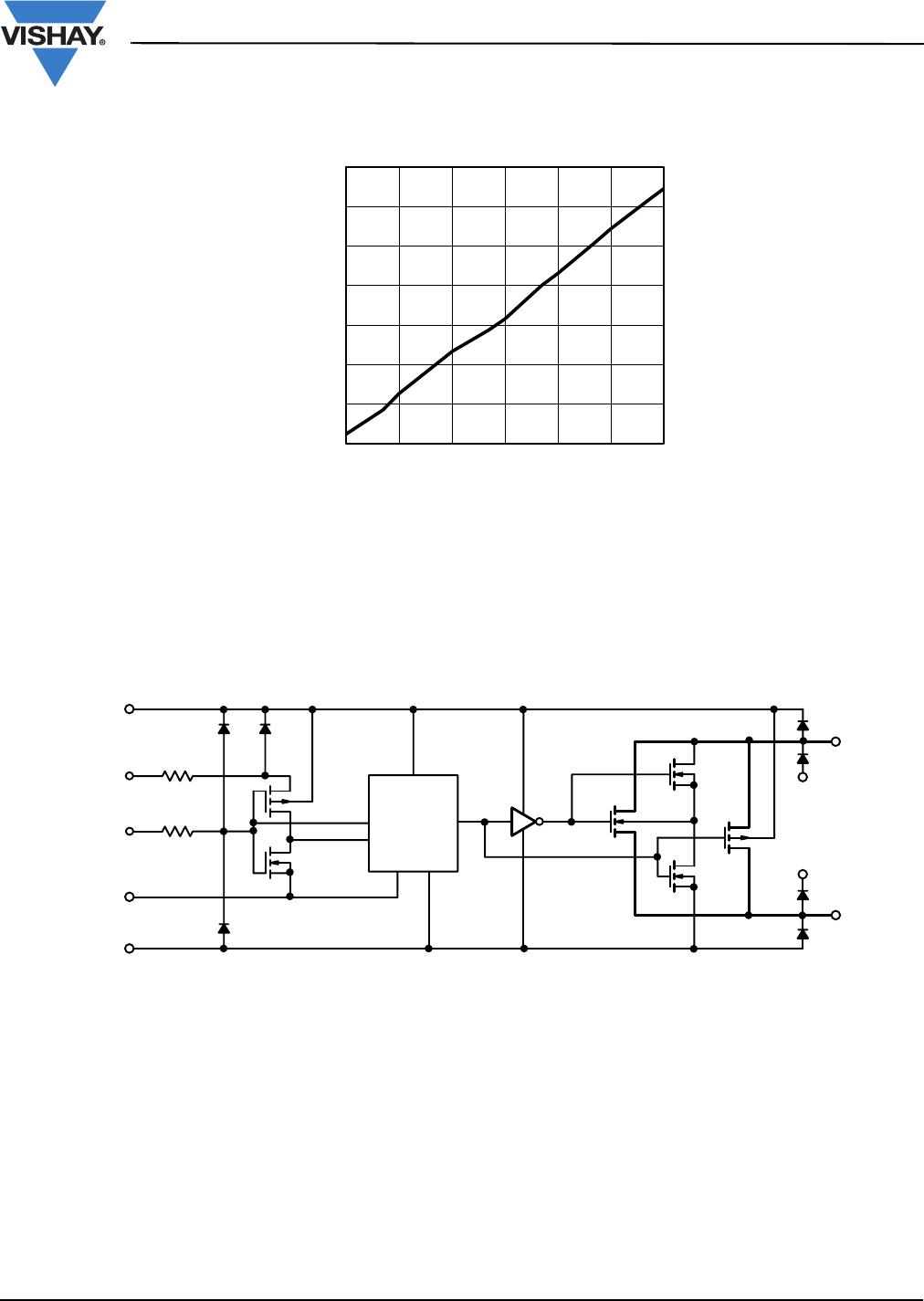
SCHEMATIC DIAGRAM
Typical Chann
el
Supply Current vs. Switching F
requency
F
requency (Hz)
Supply Current (A)
100 mA
10 mA
1 mA
100 µA
10 µA
1 µA
100 nA
10 nA
10
100
1K
10K
100K
1M
10M
Figure 1.
Level
Shift/
Drive
V
IN
V
L
S
V+
GND
V–
D
V–
V+
www.vishay.com
8
Document Number: 70049
S09-2561-Rev. I, 30-Nov-09
Vishay Siliconix
DG401, DG403, DG405
TEST CIRCUITS
V
O
is the steady state output with the sw
itch on. Feedthrough via switch capacitance
may result in spike
s at the leading and
trailing edge of
the output waveform.
Figure 2. Switching T
ime
0 V
Logic
Input
Switch
Input*
Switch
Output
0 V
Switch
Input*
V
S
t
f
< 20 ns
t
f
< 20 ns
90 %
-V
S
t
OFF
t
ON
V
O
90 %
V
O
* V
S
= 10
V for t
ON
, V
S
= - 10
V for t
OFF
Note:
Logic input wavef
or
m is inv
er
ted for s
witches that
hav
e the opposite logic sense control
C
L
(includes fixture and stra
y capacitance)
V+
IN
R
L
R
L
+ r
DS(on)
V
O
=
V
S
S
D
- 15
V
V
O
GND
± 10
V
V
L
C
L
35 pF
V-
R
L
1 k
Ω
+ 15
V
+ 5
V
50 %
Figure 3. Break-Before-Make
0 V
Logic
Input
Switch
Switch
Output
3 V
50 %
0 V
Output
0 V
90 %
V
O2
V
O1
90 %
V
S1
V
S2
t
D
t
D
V
O2
C
L
(includes fixture and stra
y capacitance)
V+
R
L1
S
2
C
L1
V-
S
1
V
L
V
S2
IN
D
2
V
S1
R
L2
L2
D
1
V
O1
C
L2
- 15
V
GND
+ 5
V
+ 15
V
Figure 4. Charge Injection
Off
On
On
IN
Δ
V
O
V
O
Q =
Δ
V
O
x C
L
C
L
10 nF
D
R
g
V
O
V+
S
V-
3 V
IN
V
L
V
g
- 15
V
GND
+ 15
V
+ 5
V
Document Number: 70049
S09-2561-Rev. I, 30-Nov-09
www.vishay.com
9
Vishay Siliconix
DG401, DG403, DG405
TEST CIRCUITS
Figure 5. Off Isolation
Figure 6. Insertion Loss
R
L
100
Ω
D
0 V, 2.4 V
V+
R
g
= 50
Ω
- 15
V
GND
V-
C
V
S
Off Isolation = 20 log
V
S
V
O
IN
V
L
V
O
+ 5
V
C
+ 15
V
S
C
C = RF bypass
R
L
100
Ω
S
V
S
V
O
0 V, 2.4 V
IN
V
L
D
R
g
= 50
Ω
+ 5
V
- 15
V
GND
V
-
C
C
+ 15
V
V+
C
C = RF bypass
Figure 7. Crosstalk
Figure 8. Capacitances
R
g
= 50
Ω
IN
0.8 V
V
L
V+
V-
X
T
ALK
Isolation = 20 log
V
S
V
O
GND
S
2
V
S
V
O
S
1
R
L
D
C = RF bypass
50
Ω
+ 15
V
- 15
V
C
C
+ 5
V
C
D
f = 1 MHz
IN
S
V
L
V+
- 15
V
GND
V
-
C
0 V
,
2.4 V
Meter
HP4192A
Impedance
Analyzer
or Equivalent
+ 5
V
C
+ 15
V
C
P1-P3
P4-P6
P7-P9
P10-P12
P13-P15
P16-P17
DG403DY-T1-E3
Mfr. #:
Buy DG403DY-T1-E3
Manufacturer:
Vishay / Siliconix
Description:
Analog Switch ICs Dual SPDT 22/25V
Lifecycle:
New from this manufacturer.
Delivery:
DHL
FedEx
Ups
TNT
EMS
Payment:
T/T
Paypal
Visa
MoneyGram
Western
Union
Products related to this Datasheet
DG403DJ-E3
DG403DY-T1-E3
DG405DY-T1-E3
DG401DJ-E3
DG405DY-E3
DG401DY-T1-E3
DG405DJ-E3
DG401DY-E3
DG405DY-T1
DG401DY-T1
DG403DY-T1
DG403DY-E3