IDT8T49N008ANLGI REVISION A FEBRUARY 13, 2014 13 ©2014 Integrated Device Technology, Inc.
IDT8T49N008I Data Sheet PROGRAMMABLE FEMTOCLOCK
®
NG LVPECL/LVDS CLOCK GENERATOR WITH 8-OUTPUTS
AC Electrical Characteristics
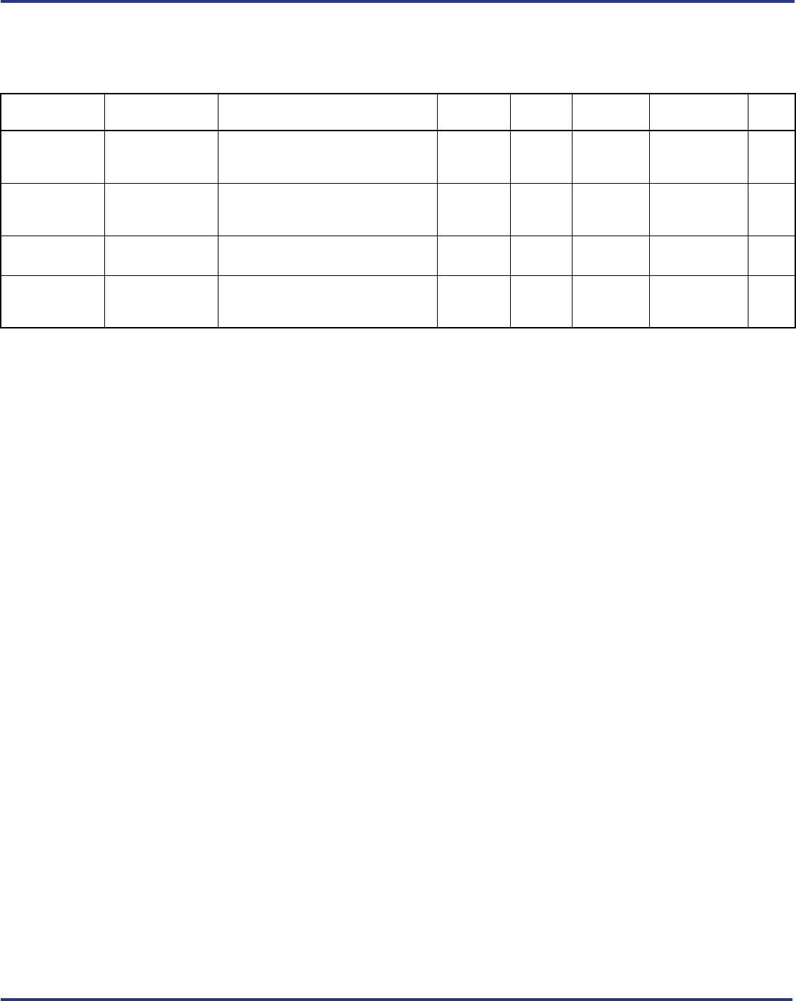
Table 6A. PCI Express Jitter Specifications, V
CC
= V
CCO
= 3.3V ± 5% or 2.5V ± 5%, V
EE
= 0V, T
A
= -40°C to 85°C
NOTE: Electrical parameters are guaranteed over the specified ambient operating temperature range, which is established when the device is
mounted in a test socket with maintained transverse airflow greater than 500 lfpm. The device will meet specifications after thermal equilibrium
has been reached under these conditions. For additional information, refer to the PCI Express Application Note section in the datasheet.
NOTE 1: Peak-to-Peak jitter after applying system transfer function for the Common Clock Architecture. Maximum limit for PCI Express Gen 1
is 86ps peak-to-peak for a sample size of 10
6
clock periods.
NOTE 2: RMS jitter after applying the two evaluation bands to the two transfer functions defined in the Common Clock Architecture and
reporting the worst case results for each evaluation band. Maximum limit for PCI Express Generation 2 is 3.1ps RMS for t
REFCLK_HF_RMS
(High Band) and 3.0ps RMS for t
REFCLK_LF_RMS
(Low Band).
NOTE 3: RMS jitter after applying system transfer function for the common clock architecture. This specification is based on the PCI Express
Base Specification Revision 0.7, October 2009 and is subject to change pending the final release version of the specification.
NOTE 4: This parameter is guaranteed by characterization. Not tested in production.
Symbol Parameter Test Conditions Minimum Typical Maximum
PCIe Industry
Specification Units
t
j
(PCIe Gen 1)
Phase Jitter
Peak-to-Peak;
NOTE 1, 4
ƒ = 100MHz, 25MHz Crystal Input
Evaluation Band: 0Hz - Nyquist
(clock frequency/2)
8.3 13.2 86 ps
t
REFCLK_HF_RMS
(PCIe Gen 2)
Phase Jitter RMS;
NOTE 2, 4
ƒ = 100MHz, 25MHz Crystal Input
High Band: 1.5MHz - Nyquist
(clock frequency/2)
0.78 1.35 3.1 ps
t
REFCLK_LF_RMS
(PCIe Gen 2)
Phase Jitter RMS;
NOTE 2, 4
ƒ = 100MHz, 25MHz Crystal Input
Low Band: 10kHz - 1.5MHz
0.05 0.10 3.0 ps
t
REFCLK_RMS
(PCIe Gen 3)
Phase Jitter RMS;
NOTE 3, 4
ƒ = 100MHz, 25MHz Crystal Input
Evaluation Band: 0Hz - Nyquist
(clock frequency/2)
0.175 0.34 0.8 ps
IDT8T49N008ANLGI REVISION A FEBRUARY 13, 2014 14 ©2014 Integrated Device Technology, Inc.
IDT8T49N008I Data Sheet PROGRAMMABLE FEMTOCLOCK
®
NG LVPECL/LVDS CLOCK GENERATOR WITH 8-OUTPUTS
Table 6B. AC Characteristics, V
CC
= V
CCO
= 3.3V ± 5% or 2.5V ± 5% V
EE
= 0V, T
A
= -40°C to 85°C
NOTE: Electrical parameters are guaranteed over the specified ambient operating temperature range, which is established when the device is
mounted in a test socket with maintained transverse airflow greater than 500 lfpm. The device will meet specifications after thermal equilibrium
has been reached under these conditions.
NOTE 1: Refer to Phase Noise Plots.
NOTE 2: Defined as skew between outputs at the same supply voltage and with equal load conditions. Measured at the differential cross
points.
NOTE 3: These parameters are guaranteed by characterization. Not tested in production.
NOTE 4: Refer to t
LOCK
and t
TRANSITION
in Parameter Measurement Information.
Symbol Parameter Test Conditions Minimum Typical Maximum Units
f
DIFF_IN
Differential Input Frequency 10 312.5 MHz
f
VCO
VCO Frequency 1910 2500 MHz
tjit(Ø)
RMS Phase Jitter, Random;
NOTE 1
25MHz Crystal, f
OUT
= 100MHz,
Integration Range:
12kHz – 20MHz
258 332 fs
25MHz Crystal, f
OUT
= 125MHz,
Integration Range: 12kHz – 20MHz
220 291 fs
25MHz Crystal, f
OUT
= 125MHz,
Integration Range: 10kHz – 1MHz
164 232 fs
25MHz Crystal, f
OUT
= 156.25MHz,
Integration Range: 12kHz – 20MHz
228 306 fs
25MHz Crystal, f
OUT
= 156.25MHz,
Integration Range: 10kHz – 1MHz
175 234 fs
25MHz Crystal, f
OUT
= 250MHz,
Integration Range: 12kHz – 20MHz
212 292 fs
30.72MHz Crystal, f
OUT
= 491.52MHz,
Integration Range: 12kHz – 20MHz
213 299 fs
19.44MHz Crystal, f
OUT
= 622.08MHz,
Integration Range: 12kHz – 20MHz
280 386 fs
tsk(o)
Output Skew;
NOTE 2, 3
LVPECL Outputs LVDS_SEL = 0 50 ps
LVDS Outputs LVDS_SEL = 1 50 ps
t
R
/ t
F
Output
Rise/Fall Time
LVPECL Outputs 20% - 80%, LVDS_SEL = 0 100 400 ps
LVDS Outputs 20% - 80%, LVDS_SEL = 1 100 400 ps
odc Output Duty Cycle
N > 3 Output Divider;
LVDS_SEL = 0 or 1
47 53 %
N 3 Output Divider;
LVDS_SEL = 0 or 1
42 58 %
t
LOCK
PLL Lock Time;
NOTE 3, 4
LOCK Output 20 ms
t
TRANSITION
Transition
Time;
NOTE 3, 4
LOCK Output 20 ms
IDT8T49N008ANLGI REVISION A FEBRUARY 13, 2014 15 ©2014 Integrated Device Technology, Inc.
IDT8T49N008I Data Sheet PROGRAMMABLE FEMTOCLOCK
®
NG LVPECL/LVDS CLOCK GENERATOR WITH 8-OUTPUTS
Typical Phase Noise at 100MHz (3.3V)
Typical Phase Noise at 125MHz (3.3V)
Noise Power (dBc/Hz)
Offset Frequency (Hz)
Noise Power (dBc/Hz)
Offset Frequency (Hz)

8T49N008A-024NLGI

Mfr. #:
Manufacturer:
IDT
Description:
Clock Generators & Support Products FEMTOCLOCK NG
Lifecycle:
New from this manufacturer.
Delivery:
DHL FedEx Ups TNT EMS
Payment:
T/T Paypal Visa MoneyGram Western Union