IRFS/SL4227PbF
2 www.irf.com
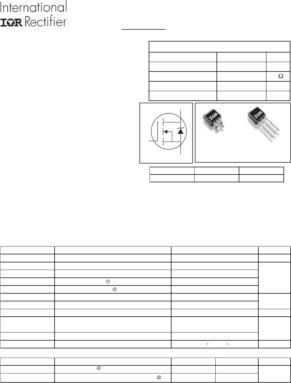
S
D
G
Electrical Characteristics @ T
J
= 25°C (unless otherwise specified)
Parameter Min. Typ. Max. Units
BV
DSS
Drain-to-Source Breakdown Voltage 200 ––– ––– V
∆Β
V
DSS
/
∆
T
J
Breakdown Voltage Temp. Coefficient ––– 170 ––– mV/°C
R
DS(on)
Static Drain-to-Source On-Resistance ––– 22 26
mΩ
V
GS(th)
Gate Threshold Voltage 3.0 ––– 5.0 V
∆V
GS(th)
/∆T
J
Gate Threshold Voltage Coefficient ––– -13 ––– mV/°C
I
DSS
Drain-to-Source Leakage Current ––– ––– 20 µA
––– ––– 200 µA
I
GSS
Gate-to-Source Forward Leakage ––– ––– 100 nA
Gate-to-Source Reverse Leakage ––– ––– -100
g
fs
Forward Transconductance 49 ––– ––– S
Q
g
Total Gate Charge ––– 70 98 nC
Q
gd
Gate-to-Drain Charge ––– 23 –––
t
d(on)
Turn-On Delay Time ––– 33 –––
t
r
Rise Time ––– 20 ––– ns
t
d(off)
Turn-Off Delay Time ––– 21 –––
t
f
Fall Time ––– 31 –––
t
st
Shoot Through Blocking Time 100 ––– ––– ns
E
PULSE
Energy per Pulse µJ
C
iss
Input Capacitance ––– 4600 –––
C
oss
Output Capacitance ––– 460 ––– pF
C
rss
Reverse Transfer Capacitance ––– 91 –––
C
oss
eff.
Effective Output Capacitance ––– 360 –––
L
D
Internal Drain Inductance ––– 4.5 ––– Between lead,
nH 6mm (0.25in.)
L
S
Internal Source Inductance ––– 7.5 ––– from package
Avalanche Characteristics
Parameter Units
E
AS
Single Pulse Avalanche Energy mJ
E
AR
Repetitive Avalanche Energy
mJ
V
DS(Avalanche)
Repetitive Avalanche Voltage V
I
AS
Avalanche Current
A
Diode Characteristics
Parameter Min. Typ. Max. Units
I
S
@ T
C
= 25°C
Continuous Source Current
(Body Diode) A
I
SM
Pulsed Source Current
(Body Diode)
V
SD
Diode Forward Voltage ––– ––– 1.3 V
t
rr
Reverse Recovery Time ––– 100 150 ns
Q
rr
Reverse Recovery Charge ––– 430 640 nC
62
260
––– –––
––– –––
MOSFET symbol
V
DS
= 25V, I
D
= 46A
V
DD
= 100V, I
D
= 46A, V
GS
= 10V
Conditions
and center of die contact
V
DD
= 160V, V
GS
= 15V, R
G
= 4.7Ω
V
DS
= 160V, R
G
= 4.7Ω, T
J
= 25°C
L = 220nH, C= 0.4µF, V
GS
= 15V
V
DS
= 160V, R
G
= 4.7Ω, T
J
= 100°C
V
DS
= 25V
V
DS
= V
GS
, I
D
= 250µA
V
DS
= 200V, V
GS
= 0V
V
GS
= 0V, V
DS
= 0V to 160V
V
DS
= 200V, V
GS
= 0V, T
J
= 125°C
V
GS
= 20V
V
GS
= -20V
V
GS
= 0V
L = 220nH, C= 0.4µF, V
GS
= 15V
Conditions
V
GS
= 0V, I
D
= 250µA
Reference to 25°C, I
D
= 1mA
V
GS
= 10V, I
D
= 46A
T
J
= 25°C, I
F
= 46A, V
DD
= 50V
di/dt = 100A/µs
T
J
= 25°C, I
S
= 46A, V
GS
= 0V
showing the
integral reverse
p-n junction diode.
Typ. Max.
ƒ = 1.0MHz,
––– 140
46
37
–––
–––
240 –––
––– 570 –––
––– 910 –––
V
DD
= 100V, V
GS
= 10V
I
D
= 46A
R
G
= 2.5Ω
See Fig. 22