Arria II Device Handbook Volume 1: Device Interfaces and Integration
July 2012
AIIGX51001-4.4
Subscribe
© 2012 Altera Corporation. All rights reserved. ALTERA, ARRIA, CYCLONE, HARDCOPY, MAX, MEGACORE, NIOS, QUARTUS and STRATIX are Reg. U.S. Pat. & Tm. Off.
and/or trademarks of Altera Corporation in the U.S. and other countries. All other trademarks and service marks are the property of their respective holders as described at
www.altera.com/common/legal.html. Altera warrants performance of its semiconductor products to current specifications in accordance with Altera’s standard warranty, but
reserves the right to make changes to any products and services at any time without notice. Altera assumes no responsibility or liability arising out of the application or use of any
information, product, or service described herein except as expressly agreed to in writing by Altera. Altera customers are advised to obtain the latest version of device
specifications before relying on any published information and before placing orders for products or services.
1. Overview for the Arria II Device Family
The Arria
®
II device family is designed specifically for ease-of-use. The
cost-optimized, 40-nm device family architecture features a low-power,
programmable logic engine and streamlined transceivers and I/Os. Common
interfaces, such as the Physical Interface for PCI Express
®
(PCIe
®
), Ethernet, and
DDR3 memory are easily implemented in your design with the Quartus
®
II software,
the SOPC Builder design software, and a broad library of hard and soft intellectual
property (IP) solutions from Altera. The Arria II device family makes designing for
applications requiring transceivers operating at up to 6.375 Gbps fast and easy.
This chapter contains the following sections:
“Arria II Device Feature” on page 1–1
“Arria II Device Architecture” on page 1–6
“Reference and Ordering Information” on page 1–14
Arria II Device Feature
The Arria II device features consist of the following highlights:
40-nm, low-power FPGA engine
Adaptive logic module (ALM) offers the highest logic efficiency in the industry
Eight-input fracturable look-up table (LUT)
Memory logic array blocks (MLABs) for efficient implementation of small
FIFOs
High-performance digital signal processing (DSP) blocks up to 550 MHz
Configurable as 9 x 9-bit, 12 x 12-bit, 18 x 18-bit, and 36 x 36-bit full-precision
multipliers as well as 18 x 36-bit high-precision multiplier
Hardcoded adders, subtractors, accumulators, and summation functions
Fully-integrated design flow with the MATLAB and DSP Builder software
from Altera
Maximum system bandwidth
Up to 24 full-duplex clock data recovery (CDR)-based transceivers supporting
rates between 600 Mbps and 6.375 Gbps
Dedicated circuitry to support physical layer functionality for popular serial
protocols, including PCIe Gen1 and PCIe Gen2, Gbps Ethernet, Serial
RapidIO
®
(SRIO), Common Public Radio Interface (CPRI), OBSAI,
SD/HD/3G/ASI Serial Digital Interface (SDI), XAUI and Reduced XAUI
(RXAUI), HiGig/HiGig+, SATA/Serial Attached SCSI (SAS), GPON,
SerialLite II, Fiber Channel, SONET/SDH, Interlaken, Serial Data Converter
(JESD204), and SFI-5.
July 2012
AIIGX51001-4.4
1–2 Chapter 1: Overview for the Arria II Device Family
Arria II Device Feature
Arria II Device Handbook Volume 1: Device Interfaces and Integration July 2012 Altera Corporation
Complete PIPE protocol solution with an embedded hard IP block that provides
physical interface and media access control (PHY/MAC) layer, Data Link layer,
and Transaction layer functionality
Optimized for high-bandwidth system interfaces
Up to 726 user I/O pins arranged in up to 20 modular I/O banks that support a
wide range of single-ended and differential I/O standards
High-speed LVDS I/O support with serializer/deserializer (SERDES) and
dynamic phase alignment (DPA) circuitry at data rates from 150 Mbps to
1.25 Gbps
Low power
Architectural power reduction techniques
Typical physical medium attachment (PMA) power consumption of 100 mW at
3.125 Gbps.
Power optimizations integrated into the Quartus II development software
Advanced usability and security features
Parallel and serial configuration options
On-chip series (R
S
) and on-chip parallel (R
T
) termination with auto-calibration
for single-ended I/Os and on-chip differential (R
D
) termination for differential
I/O
256-bit advanced encryption standard (AES) programming file encryption for
design security with volatile and non-volatile key storage options
Robust portfolio of IP for processing, serial protocols, and memory interfaces
Low cost, easy-to-use development kits featuring high-speed mezzanine
connectors (HSMC)
Emulated LVDS output support with a data rate of up to 1152 Mbps
Chapter 1: Overview for the Arria II Device Family 1–3
Arria II Device Feature
July 2012 Altera Corporation Arria II Device Handbook Volume 1: Device Interfaces and Integration
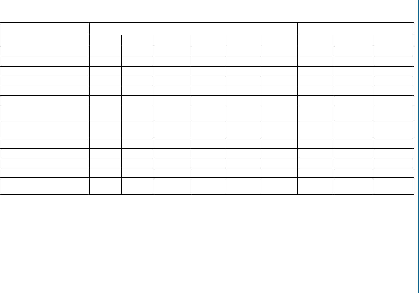
Table 1–1 lists the Arria II device features.
Table 1–1. Features in Arria II Devices
Feature
Arria II GX Devices Arria II GZ Devices
EP2AGX45 EP2AGX65 EP2AGX95 EP2AGX125 EP2AGX190 EP2AGX260 EP2AGZ225 EP2AGZ300 EP2AGZ350
Total Transceivers (1) 8 8 12 12 16 16 16 or 24 16 or 24 16 or 24
ALMs 18,050 25,300 37,470 49,640 76,120 102,600 89,600 119,200 139,400
LEs 42,959 60,214 89,178 118,143 181,165 244,188 224,000 298,000 348,500
PCIe hard IP blocks 1 1 1 1 1 1 1 1 1
M9K Blocks 319 495 612 730 840 950 1,235 1,248 1,248
M144K Blocks 24 36
Total Embedded Memory in M9K
Blocks (Kbits)
2,871 4,455 5,508 6,570 7,560 8,550 11,115 14,688 16,416
Total On-Chip Memory
(M9K +M144K + MLABs) (Kbits)
3,435 5,246 6,679 8,121 9,939 11,756 13,915 18,413 20,772
Embedded Multipliers (18 x 18) (2) 232 312 448 576 656 736 800 920 1,040
General Purpose PLLs 4 4 6 6 6 6 6 or 8 4, 6, or 8 4, 6, or 8
Transceiver TX PLLs (3), (4) 2 or 4 2 or 4 4 or 6 4 or 6 6 or 8 6 or 8 8 or 12 8 or 12 8 or 12
User I/O Banks (5), (6) 6 6 8 8 12 12 16 or 20 8, 16, or 20 8, 16, or 20
High-Speed LVDS SERDES
(up to 1.25 Gbps) (7)
8, 24, or 28 8, 24, or 28 24, 28, or 32 24, 28, 32 28 or 48 24 or 48 42 or 86 0 (8), 42, or 86 0 (8), 42, or 86
Notes to Table 1–1:
(1) The total number of transceivers is divided equally between the left and right side of each device, except for the devices in the F780 package. These devices have eight transceiver channels located only on
the right side of the device.
(2) This is in four multiplier adder mode.
(3) The FPGA fabric can use these phase locked-loops (PLLs) if they are not used by the transceiver.
(4) The number of PLLs depends on the package. Transceiver transmitter (TX) PLL count = (number of transceiver blocks)
× 2.
(5) Banks 3C and 8C are dedicated configuration banks and do not have user I/O pins.
(6) For Arria II GZ devices, the user I/Os count from pin-out files includes all general purpose I/O, dedicated clock pins, and dual purpose configuration pins. Transceiver pins and dedicated configuration pins
are not included in the pin count.
(7) For Arria II GZ devices, total pairs of high-speed LVDS SERDES take the lowest channel count of RX/TX. For more information, refer to the High-Speed I/O Interfaces and DPA in Arria II Devices chapter.
(8) The smallest pin package (780-pin package) does not support high-speed LVDS SERDES.

EP2AGX95EF29C5G

Mfr. #:
Manufacturer:
Intel / Altera
Description:
FPGA - Field Programmable Gate Array
Lifecycle:
New from this manufacturer.
Delivery:
DHL FedEx Ups TNT EMS
Payment:
T/T Paypal Visa MoneyGram Western Union