Chapter 1: Overview for the Arria II Device Family 1–7
Arria II Device Architecture
July 2012 Altera Corporation Arria II Device Handbook Volume 1: Device Interfaces and Integration
High-Speed Transceiver Features
Arria II GX devices integrate up to 16 transceivers and Arria II GZ devices up to
24 transceivers on a single device. The transceiver block is optimized for cost and
power consumption. Arria II transceivers support the following features:
Configurable pre-emphasis and equalization, and adjustable output differential
voltage
Flexible and easy-to-configure transceiver datapath to implement proprietary
protocols
Signal integrity features
Programmable transmitter pre-emphasis to compensate for inter-symbol
interference (ISI)
User-controlled receiver equalization with up to 7 dB (Arria II GX) and
16 dB (Arria II GZ) of high-frequency gain
On-die power supply regulators for transmitter and receiver PLL charge pump
and voltage-controlled oscillator (VCO) for superior noise immunity
Calibration circuitry for transmitter and receiver on-chip termination (OCT)
resistors
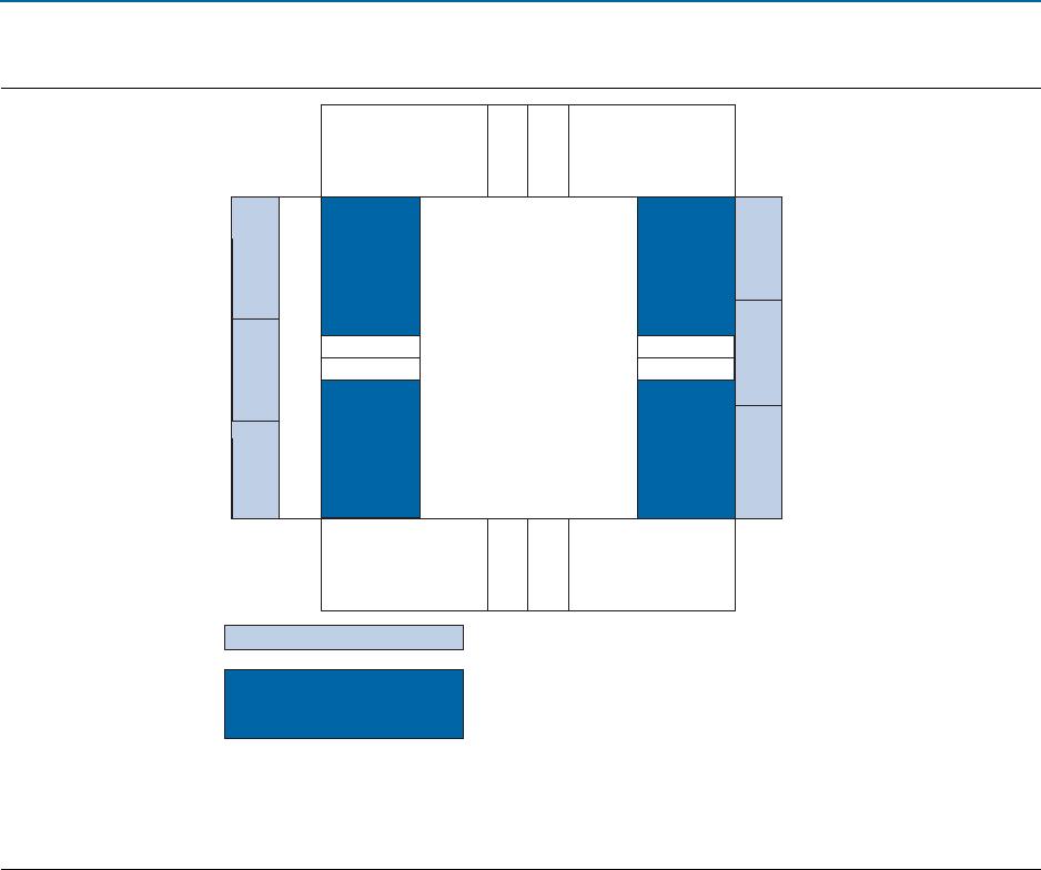
Figure 1–2. Architecture Overview for Arria II GZ Device
Notes to Figure 1–2:
(1) Not available for 780-pin FBGA package.
(2) Not available for 780-pin and 1152-pin FBGA packages.
(3) The PCIe hard IP block is located on the left side of the device only (IOBANK_QL).
General Purpose
I/O and Memory
Interface
400 Mbps-6.375 Gbps CDR-based Transceiver
General Purpose I/O and 150 Mbps-1.25 Gbps
LVDS interface with DPA and Soft-CDR
Transceiver
Block
Transceiver
Block
Transceiver
Block
PCIe hard IP Block
(3)
General Purpose
I/O and Memory
Interface
PLL
(2)
PLL
(1)
PLL PLL
General Purpose
I/O and Memory
Interface
General Purpose
I/O and Memory
Interface
PLL PLL
Arria II GZ FPGA Fabric
(Logic Elements, DSP,
Embedded Memory,
Clock Networks)
Transceiver Block
General Purpose I/O and
High-Speed LVDS I/O
with DPA and Soft CDR
General Purpose
I/O and
High-Speed
LVDS I/O with
DPA and Soft CDR
PLL
(2)
PLL
(1)
Transceiver
Block
Transceiver
Block
Transceiver
Block
General Purpose
I/O and
High-Speed
LVDS I/O with
DPA and Soft CDR
General Purpose
I/O and
High-Speed
LVDS I/O with
DPA and Soft CDR
General Purpose
I/O and
High-Speed
LVDS I/O with
DPA and Soft CDR
1–8 Chapter 1: Overview for the Arria II Device Family
Arria II Device Architecture
Arria II Device Handbook Volume 1: Device Interfaces and Integration July 2012 Altera Corporation
Diagnostic features
Serial loopback from the transmitter serializer to the receiver CDR for
transceiver physical coding sublayer (PCS) and PMA diagnostics
Parallel loopback from the transmitter PCS to the receiver PCS with built-in self
test (BIST) pattern generator and verifier
Reverse serial loopback pre- and post-CDR to transmitter buffer for physical
link diagnostics
Loopback master and slave capability in PCIe hard IP blocks
Support for protocol features such as MSB-to-LSB transmission in a
SONET/SDH configuration and spread-spectrum clocking in a PCIe
configuration
Table 15 lists common protocols and the Arria II dedicated circuitry and features for
implementing these protocols.
1 For other protocols supported by Arria II devices, such as SONET/SDH, SDI, SATA
and SRIO, refer to the Transceiver Architecture in Arria II Devices chapter.
Table 1–5. Sample of Supported Protocols and Feature Descriptions for Arria II Devices
Supported Protocols Feature Descriptions
PCIe
Complete PCIe Gen1 and Gen2 protocol stack solution compliant to PCIe Base
Specification 2.0 that includes PHY/MAC, Data Link, and Transaction layer circuitry
embedded in the PCIe hard IP blocks.
PCIe Gen1 has x1, x2, x4, and x8 lane configurations. PCIe Gen2 has x1, x2, and x4 lane
configurations. PCIe Gen2 does not support x8 lane configurations
Built-in circuitry for electrical idle generation and detection, receiver detect, power state
transitions, lane reversal, and polarity inversion
8B/10B encoder and decoder, receiver synchronization state machine, and ±300 parts
per million (PPM) clock compensation circuitry
Options to use:
Hard IP Data Link Layer and Transaction Layer
Hard IP Data Link Layer and custom Soft IP Transaction Layer
XAUI/HiGig/HiGig+
Compliant to IEEE P802.3ae specification
Embedded state machine circuitry to convert XGMII idle code groups (||I||) to and from
idle ordered sets (||A||, ||K||, ||R||) at the transmitter and receiver, respectively
8B/10B encoder and decoder, receiver synchronization state machine, lane deskew, and
±100 PPM clock compensation circuitry
GbE
Compliant to IEEE 802.3 specification
Automatic idle ordered set (/I1/, /I2/) generation at the transmitter, depending on the
current running disparity
8B/10B encoder and decoder, receiver synchronization state machine, and ±100 PPM
clock compensation circuitry
CPRI/OBSAI
Transmit bit slipper eliminates latency uncertainty to comply with CPRI/OBSAI
specifications
Optimized for power and cost for remote radio heads and RF modules
Chapter 1: Overview for the Arria II Device Family 1–9
Arria II Device Architecture
July 2012 Altera Corporation Arria II Device Handbook Volume 1: Device Interfaces and Integration
1 PCIe Gen2 protocol is only available in Arria II GZ devices.
The following sections provide an overview of the various features of the Arria II
FPGA.
PCIe Hard IP Block
Every Arria II device includes an integrated hard IP block which implements PCIe
PHY/MAC, data link, and transaction layers. This PCIe hard IP block is highly
configurable to meet the requirements of the majority of PCIe applications. PCIe
hard IP makes implementing PCIe Gen1 and PCIe Gen2 solution in your Arria II
design simple and easy.
You can instantiate PCIe hard IP block using the PCI Compiler MegaWizard
TM
Plug-In Manager, similar to soft IP functions, but does not consume core FPGA
resources or require placement, routing, and timing analysis to ensure correct
operation of the core. Table 1–6 lists the PCIe hard IP block support for Arria II GX
and GZ devices.
Logic Array Block and Adaptive Logic Modules
Logic array blocks (LABs) consists of 10 ALMs, carry chains, shared arithmetic
chains, LAB control signals, local interconnect, and register chain connection lines
ALMs expand the traditional four-input LUT architecture to eight-inputs,
increasing performance by reducing logic elements (LEs), logic levels, and
associated routing
LABs have a derivative called MLAB, which adds SRAM-memory capability to
the LAB
MLAB and LAB blocks always coexist as pairs, allowing up to 50% of the logic
(LABs) to be traded for memory (MLABs)
Embedded Memory Blocks
MLABs, M9K, and M144K embedded memory blocks provide up to 20,836 Kbits
of on-chip memory capable of up to 540-MHz performance. The embedded
memory structure consists of columns of embedded memory blocks that you can
configure as RAM, FIFO buffers, and ROM.
Optimized for applications such as high-throughput packet processing,
high-definition (HD) line buffers for video processing functions, and embedded
processor program and data storage.
Table 1–6. PCIe Hard IP Block Support
Support Arria II GX Devices Arria II GZ Devices
PCIe Gen1 x1, x4, x8 x1, x4, x8
PCIe Gen2 x1, x4
Root Port and endpoint configurations Yes Yes
Payloads 128-byte to 256-byte 128-byte to 2K-byte

EP2AGX95EF29C5G

Mfr. #:
Manufacturer:
Intel / Altera
Description:
FPGA - Field Programmable Gate Array
Lifecycle:
New from this manufacturer.
Delivery:
DHL FedEx Ups TNT EMS
Payment:
T/T Paypal Visa MoneyGram Western Union