X9317
4
FN8183.9
November 4, 2014
Submit Document Feedback
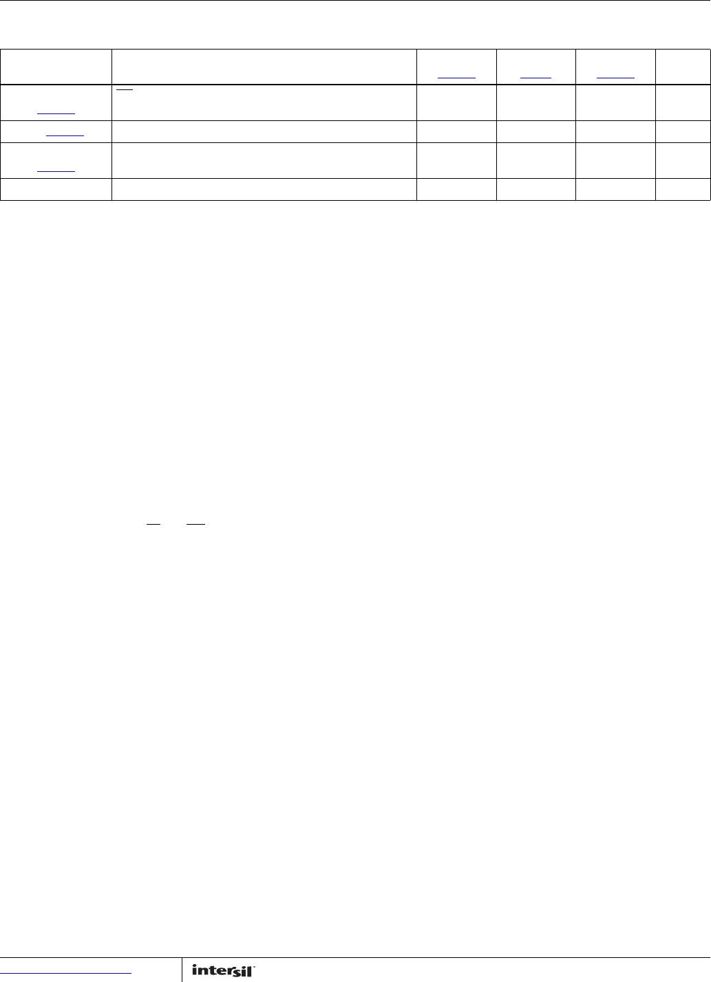
Absolute Maximum Ratings Thermal Information
I
W
(10s) . . . . . . . . . . . . . . . . . . . . . . . . . . . . . . . . . . . . . . . . . . . . . . . . .±8.8mA
R
H
, R
W
, R
L
to Ground . . . . . . . . . . . . . . . . . . . . . . . . . . . . . . . . . . . . . . . . . +6V
Voltage on CS
, INC, U/D and V
CC
with Respect to V
SS
. . . . . . . . . . . . . . . . . . . . . . . . . . . . . . . . . . .-1V to +7V
Thermal Resistance (Typical)
JA
(°C/W)
JC
(°C/W)
SOIC Package (Notes 4
, 5) . . . . . . . . . . . . . 115 60
MSOP Package (Notes 4
, 5) . . . . . . . . . . . . 145 55
TSSOP Package (Notes 4
, 5). . . . . . . . . . . . 155 49
Junction Temperature Under Bias . . . . . . . . . . . . . . . . . . . -65C to +135C
Storage Temperature . . . . . . . . . . . . . . . . . . . . . . . . . . . . . .-65°C to +150°C
Pb-Free Reflow Profile . . . . . . . . . . . . . . . . . . . . . . . . . . . . . . . . . . see TB493
CAUTION: Do not operate at or near the maximum ratings listed for extended periods of time. Exposure to such conditions may adversely impact product
reliability and result in failures not covered by warranty.
NOTES:
4.
JA
is measured with the component mounted on a high effective thermal conductivity test board in free air. See Tech Brief TB379 for details.
5. For
JC
, the “case temp” location is taken at the package top center.
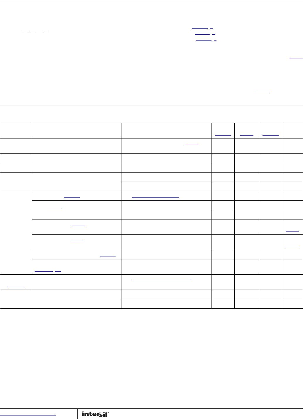
Potentiometer Specifications V
CC
= full range. Boldface limits apply across the operating temperature range, -40°C to +85°C
(Industrial) and 0°C to +70°C (Commercial).
SYMBOL PARAMETER TEST CONDITIONS/NOTES
MIN
(Note 13
)
TYP
(Note 9)
MAX
(Note 13)UNIT
R
TOTAL
End-to-end Resistance Tolerance See “Ordering Information” on page 2 for
values
-20 +20 %
V
RH
/
RL
R
H
/R
L
Terminal Voltage V
SS
= 0V V
SS
V
CC
V
Power Rating R
TOTAL
10kΩ 10 mW
R
W
Wiper Resistance I
W
= [V(R
H
) - V(R
L
)]/ R
TOTAL
, V
CC
= 5V 200 400 Ω
I
W
= [V(R
H
) - V(R
L
)]/ R
TOTAL
, V
CC
= 2.7V 400 1000 Ω
I
W
Wiper Current
(Note 10) See Test Circuit” on page 5 -4.4 +4.4 mA
Noise
(Note 12) Ref: 1kHz -120 dBV
Resolution 1%
Absolute Linearity (Note 6
)V(R
H
) = V
CC
, V(R
L
) = 0V -1 +1 MI
(Note 8)
Relative Linearity (Note 7)V(R
H
) = V
CC
, V(R
L
) = 0V -0.2 +0.2 MI
(Note 8
)
R
TOTAL
Temperature Coefficient
(Note 10)V(R
H
) = V
CC
, V(R
L
) = 0V ±300 ppm/°C
Ratiometric Temperature Coefficient
(Notes 10
, 11)
±20 ppm/°C
C
H
/C
L
/C
W
(Note 10)
Potentiometer Capacitances See
Equivalent Circuit” on page 5 10/10/25 pF
V
CC
Supply Voltage X9317 4.5 5.5 V
X9317-2.7 2.7 5.5 V
X9317
5
FN8183.9
November 4, 2014
Submit Document Feedback
DC Electrical Specifications V
CC
= 5V ±10%. Boldface limits apply across the operating temperature range, -40°C to +85°C
(Industrial) and 0°C to +70°C (Commercial).
SYMBOL PARAMETER TEST CONDITIONS
MIN
(Note 13
)
TYP
(Note 9)
MAX
(Note 13)UNIT
I
CC1
V
CC
Active Current (Increment) CS = V
IL
, U/D = V
IL
or V
IH
and INC =V
IL
/V
IH
at
min. t
CYC
R
L
, R
H
, R
W
not connected
80 µA
I
CC2
V
CC
Active Current (Store)
(non-volatile write)
CS = V
IH
, U/D = V
IL
or V
IH
and INC = V
IL
or V
IH
.
R
L
, R
H
, R
W
not connected
400 µA
I
SB
Standby Supply Current CS V
IH
, U/D and INC =V
IL
R
L
, R
H
, R
W
not connected
5 µA
I
LI
CS, INC, U/D Input Leakage Current V
IN
= V
SS
to V
CC
-10 +10 µA
V
IH
CS, INC, U/D Input HIGH Voltage V
CC
x 0.7 V
CC
+ 0.5 V
V
IL
CS, INC, U/D Input LOW Voltage -0.5 V
CC
x 0.1 V
C
IN
(Note 10)CS, INC, U/D Input Capacitance V
CC
= 5V, V
IN
= V
SS
, T
A
= +25°C, f = 1MHz 10 pF
Endurance and Data Retention V
CC
= 5V ±10%, T
A
= Full Operating Temperature Range.
PARAMETER MIN UNIT
Minimum Endurance 100,000 Data changes per bit
Data Retention 100 Years
Test Circuit Equivalent Circuit
FORCE
CURRENT
TEST POINT
R
W
C
H
C
L
R
W
10pF
10pF
R
TOTAL
C
W
25pF
R
H
R
L
AC Conditions of Test
Input pulse levels 0V to 3V
Input rise and fall times 10ns
Input reference levels 1.5V
AC Electrical Specifications V
CC
= 5V ±10%. Boldface limits apply across the operating temperature range, -40°C to +85°C
(Industrial) and 0°C to +70°C (Commercial).
SYMBOL PARAMETER
MIN
(Note 13
)
TYP
(Note 9)
MAX
(Note 13)UNIT
t
Cl
CS to INC Setup 50 ns
t
lD
(Note 10)INC HIGH to U/D Change 100 ns
t
DI
(Note 10)U/D to INC Setup 1 µs
t
lL
INC LOW Period 960 ns
t
lH
INC HIGH Period 960 ns
t
lC
INC Inactive to CS Inactive 1 µs
t
CPHS
CS Deselect Time (STORE) 10 ms
t
CPHNS
(Note 10)
CS
Deselect Time (NO STORE) 100 ns
t
IW
INC to R
W
Change 1 5 µs
t
CYC
INC Cycle Time 2 µs
X9317
6
FN8183.9
November 4, 2014
Submit Document Feedback
Power-up and Down
Requirements
The recommended power-up sequence is to apply V
CC
/V
SS
first,
then the potentiometer voltages. During power-up, the data sheet
parameters for the DCP do not fully apply until 1ms after V
CC
reaches its final value. The V
CC
ramp spec is always in effect. In
order to prevent unwanted tap position changes, or an
inadvertent store, bring the CS
and INC high before or
concurrently with the V
CC
pin on power-up.
t
R,
t
F
(Note 10)
INC
Input Rise and Fall Time 500 µs
t
PU
(Note 10) Power-up to Wiper Stable 5 µs
t
R
V
CC
(Note 10)
V
CC
Power-up Rate 0.2 50 V/ms
t
WR
Store Cycle 5 10 ms
NOTES:
6. Absolute linearity is utilized to determine actual wiper voltage versus expected voltage = [V(R
W(n)(actual)
)-V(R
W(n)(expected)
)]/MI
V(R
W(n)(expected)
) = n(V(R
H
)-V(R
L
))/99 + V(R
L
), with n from 0 to 99.
7. Relative linearity is a measure of the error in step size between taps = [V(R
W(n+1)
)-(V(R
W(n)
) - MI)]/MI.
8. 1 Ml = Minimum Increment = [V(R
H
)-V(R
L
)]/99.
9. Typical values are for T
A
= +25°C and nominal supply voltage.
10. This parameter is not 100% tested.
11. Ratiometric temperature coefficient = (V(R
W
)
T1(n)
-V(R
W
)
T2(n)
)/[V(R
W
)
T1(n)
(T1-T2) x 10
6
], with T1 and T2 being 2 temperatures, and n from 0 to 99.
12. Measured with wiper at tap position 99, R
L
grounded, using test circuit.
13. Parameters with MIN and/or MAX limits are 100% tested at +25°C, unless otherwise specified. Temperature limits established by characterization
and are not production tested.
AC Electrical Specifications V
CC
= 5V ±10%. Boldface limits apply across the operating temperature range, -40°C to +85°C
(Industrial) and 0°C to +70°C (Commercial). (Continued)
SYMBOL PARAMETER
MIN
(Note 13
)
TYP
(Note 9)
MAX
(Note 13)UNIT

X9317WM8IZ-2.7

Mfr. #:
Manufacturer:
Renesas / Intersil
Description:
Digital Potentiometer ICs SINGLE XDCP 10KOHM 100 TAP U/D
Lifecycle:
New from this manufacturer.
Delivery:
DHL FedEx Ups TNT EMS
Payment:
T/T Paypal Visa MoneyGram Western Union