X9317
8
FN8183.9
November 4, 2014
Submit Document Feedback
Pin Descriptions
R
H
and R
L
The high (R
H
) and low (R
L
) terminals of the X9317 are equivalent
to the fixed terminals of a mechanical potentiometer. The
terminology of R
L
and R
H
references the relative position of the
terminal in relation to wiper movement direction selected by the
U/D
input and not the voltage potential on the terminal.
R
W
R
W
is the wiper terminal and is equivalent to the movable
terminal of a mechanical potentiometer. The position of the
wiper within the array is determined by the control inputs. The
wiper terminal series resistance is typically 200Ω.
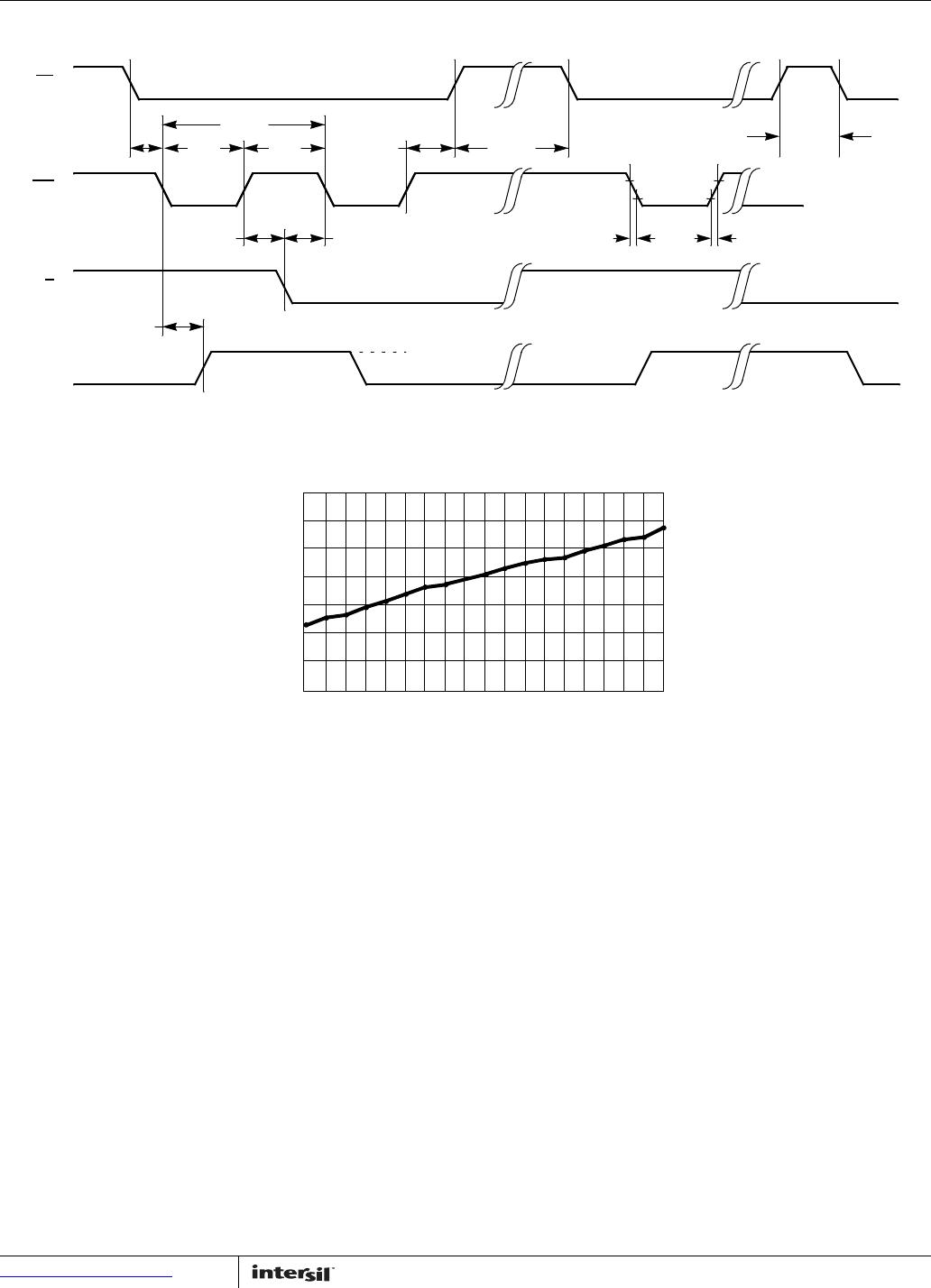
Up/Down (U/D)
The U/D input controls the direction of the wiper movement and
whether the counter is incremented or decremented.
Increment (INC)
The INC input is negative-edge triggered. Toggling INC will move
the wiper and either increment or decrement the counter in the
direction indicated by the logic level on the U/D
input.
Chip Select (CS)
The device is selected when the CS input is LOW. The current
counter value is stored in nonvolatile memory when CS is
returned HIGH while the INC input is also HIGH. After the store
operation is complete, the X9317 will be placed in the low power
standby mode until the device is selected once again.
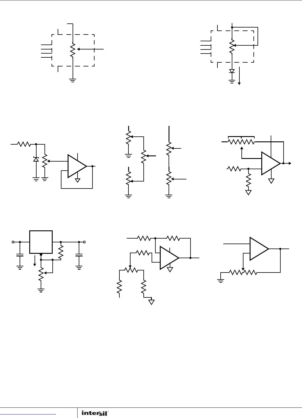
Principles of Operation
There are three sections of the X9317: the control section, the
nonvolatile memory, and the resistor array. The control section
operates just like an up/down counter. The output of this counter
is decoded to turn on a single electronic switch connecting a
point on the resistor array to the wiper output. The contents of the
counter can be stored in nonvolatile memory and retained for
future use. The resistor array is comprised of 99 individual
resistors connected in series. Electronic switches at either end of
the array and between each resistor provide an electrical
connection to the wiper pin, R
W
.
The wiper acts like its mechanical equivalent and does not move
beyond the first or last position. That is, the counter does not
wrap around when clocked to either extreme.
The electronic switches on the device operate in a “make before
break” mode when the wiper changes tap positions. If the wiper
is moved several positions, multiple taps are connected to the
wiper for t
IW
(INC to V
W
change). The R
TOTAL
value for the device
can temporarily be reduced by a significant amount if the wiper
is moved several positions.
When the device is powered-down, the last wiper position stored
will be maintained in the nonvolatile memory. When power is
restored, the contents of the memory are recalled and the wiper
is set to the value last stored.
Instructions and Programming
The INC, U/D and CS inputs control the movement of the wiper
along the resistor array. With CS
set LOW, the device is selected
and enabled to respond to the U/D and INC inputs. HIGH-to-LOW
transitions on INC will increment or decrement (depending on the
state of the U/D
input) a 7-bit counter. The output of this counter
is decoded to select one of one hundred wiper positions along
the resistive array.
The value of the counter is stored in nonvolatile memory
whenever CS
transitions HIGH while the INC input is also HIGH.
The system may select the X9317, move the wiper and deselect
the device without having to store the latest wiper position in
nonvolatile memory. After the wiper movement is performed as
previously described and once the new position is reached, the
system must keep INC LOW while taking CS HIGH. The new wiper
position will be maintained until changed by the system or until a
power-up/down cycle recalls the previously stored data.
This procedure allows the system to always power-up to a preset
value stored in nonvolatile memory; then during system
operation minor adjustments could be made. The adjustments
might be based on user preference, system parameter changes
due to temperature drift, etc.
The state of U/D
may be changed while CS remains LOW. This
allows the host system to enable the device and then move the
wiper up and down until the proper trim is attained.
Applications Information
Electronic digitally controlled (XDCP) potentiometers provide
three powerful application advantages:
1. The variability and reliability of a solid-state potentiometer,
2. The flexibility of computer-based digital controls, and
3. The retentivity of nonvolatile memory used for the storage of
multiple potentiometer settings or data.
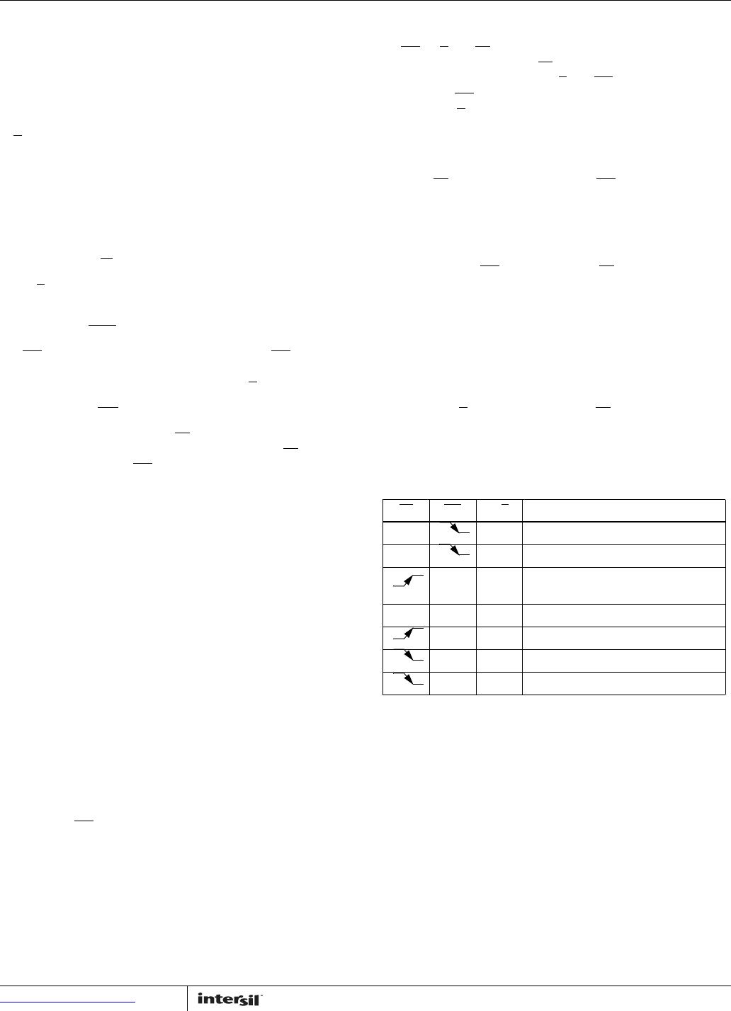
Mode Selection
CS INC U/D MODE
LHWiper up
L L Wiper down
H X Store wiper position to nonvolatile
memory
HXXStandby
L X No store, return to standby
L H Wiper up (not recommended)
L L Wiper down (not recommended)