AD8344
Rev. 0 | Page 12 of 20
04826-0-051
0180
30
330
60
90
270
300
120
240
150
210
1.2GHz
400MHz
Figure 29. RFIN Return Loss vs. RF Frequency
0
–45
–40
–35
–30
–25
–20
–15
–10
–5
400 500 600 700 800 900 1000 1100 1200
04826-0-053
RF FREQUENCY (MHz)
FEEDTHROUGH (dBc)
Figure 30. RF to IF Feedthrough vs. RF Frequency,
F
LO
= 1090 MHz, RF Power = −10 dBm
0
–80
–70
–60
–50
–40
–30
–20
–10
400 600 800 1000 1200 1400 1600
04826-0-055
LO FREQUENCY (MHz)
LEAKAGE (dBc)
Figure 31. LO to RF Leakage vs. LO Frequency, LO Power = 0 dBm
04826-0-052
0180
30
330
60
90
270
300
120
240
150
210
400MHz
1.6GHz
Figure 32. LOIN Return Loss vs. LO Frequency
0
–40
–35
–30
–25
–20
–15
–10
–5
400 600 800 1000 1200 1400 1600
04826-0-054
LO FREQUENCY (MHz)
FEEDTHROUGH (dBc)
Figure 33. LO to IF Feedthrough vs. LO Frequency, LO Power = 0 dBm
14000
12000
10000
8000
6000
4000
2000
3.0
2.5
2.0
1.5
1.0
0.5
0
70 370320270220170120
04826-0-030
FREQUENCY (MHz)
RESISTANCE ()
CAPACITANCE (pF)
Figure 34. IF Port Output Resistance and Capacitance vs. IF Frequency
AD8344
Rev. 0 | Page 13 of 20
e
CIRCUIT DESCRIPTION
The AD8344 is a down converting mixer optimized for opera-
tion within the input frequency range of 400 MHz to 1.2 GHz. It
has a single-ended, 50 Ω RF input, as well as a single-ended,
50 Ω local oscillator (LO) input. The IF outputs are differential
open collectors. The mixer current can be adjusted by the value
of an external resistor to optimize performance for gain com-
pression and intermodulation or for low power operation.
Figure 35 shows the basic blocks of the mixer, which includes
the LO buffer, RF voltage-to-current converter, bias cell, and
mixing core.
The RF voltage to RF current conversion is done via an
inductively degenerated differential pair. When one side of the
differential pair is ac grounded, the other input can be driven
single-ended. The RF inputs can also be driven differentially.
The voltage-to-current converter then drives the emitters of a
four-transistor switching core. This switching core is driven by
an amplified version of the local oscillator signal connected to
the LO input. There are three limiting gain stages between the
external LO signal and the switching core. The first stage con-
verts the single-ended LO drive to a well balanced differential
drive. The differential drive then passes through two more gain
stages, which ensures a limited signal drives the switching core.
This affords the user a lower LO drive requirement, while
maintaining excellent distortion and compression performance.
The output signal of these three LO gain stages drives the four
transistors within the mixer core to commutate at the rate of th
local oscillator frequency. The output of the mixer core is taken
directly from these open collectors. The open collector outputs
present a high impedance at the IF frequency. The conversion
gain of the mixer depends directly on the impedance presented
to these open collectors. In characterization, a 200 Ω load was
presented to the part via a 4:1 impedance transformer.
The AD8344 also features a power-down function.
Application of a logic low at the PWDN pin allows normal
operation. A high logic level at the PWDN pin shuts down the
AD8344. Power consumption when the part is disabled is less
than 10 mW.
The bias for the mixer is set with an external resistor from the
EXRB pin to ground. The value of this resistor directly affects
the dynamic range of the mixer. The external resistor should not
be lower than 2.4 kΩ. Permanent damage to the part will result
if values below 2.4 kΩ are used.
04826-0-003
LO
INPUT
VPLO
IFOP
IFOM
RFIN
VPMX
RFCM
BIAS
EXTERNAL
BIAS
RESISTORVPDC PWDN
SE
TO
DIFF
Figure 35. AD8344 Simplified Schematic
As shown in Figure 36, the IF output pins, IFOP and IFOM, are
directly connected to the open collectors of the NPN transistors
in the mixer core so the differential and single-ended imped-
ances looking into this port are relatively high, on the order of
several kΩ. A connection between the supply voltage and these
output pins is required for proper mixer core operation.
04826-0-003
IFOP IFOM
LOIN
RFCMRFIN
COMM
Figure 36. Mixer Core Simplified Schematic
The AD8344 has three pins for the supply voltage: VPDC,
VPMX, and VPLO. These pins are separated to minimize or
eliminate possible parasitic coupling paths within the AD8344
that could cause spurious signals or reduced interport isolation.
Consequently, each of these pins should be well bypassed and
decoupled as close to the AD8344 as possible.
AD8344
Rev. 0 | Page 14 of 20
AC INTERFACES
The AD8344 is a high-side downconverter. It is designed to
downconvert radio frequencies (RF) to lower intermediate
frequencies (IF) using a high-side local oscillator (LO). The LO
is injected into the mixer core at a frequency greater than the
desired input RF frequency. The difference between the LO and
RF frequencies, f
LO
− f
RF,
is the IF frequency, f
IF
. In addition to
the desired RF signal, an RF image will be downconverted to the
same IF frequency. The image frequency is at f
LO
+ f
IF
. The con-
version gain of the AD8344 decreases with increasing input
frequency. By choosing to use a high-side LO the image fre-
quency at f
LO
+ f
IF
is translated with less conversion gain than
the desired RF signal at f
LO
− f
IF
. Additionally, any wideband
noise present at the image frequency will be downconverted
with less conversion gain than would be the case if a low-side
LO was applied. In general, a high-side LO should be used with
the AD8344 to ensure optimal noise performance and image
rejection.
The AD8344 is designed to operate using RF frequencies in the
400 MHz to 1200 MHz frequency range, with high-side LO
injection within the 470 MHz to 1600 MHz range. It is essential
to ac-couple RF and LO ports to prevent dc offsets from skew-
ing the mixer core in an asymmetrical manner, potentially
degrading linear input swing and impacting distortion and
input compression characteristics.
The AD8344 RFIN port presents a 50 Ω impedance relative to
RFCM. In order to ensure a good impedance match, the RFIN
ac-coupling capacitor should be large enough in value so that
the presented reactance is negligible at the intended RF fre-
quency. Additionally, the RFCM bypassing capacitor should be
sufficiently large to provide a low impedance return path to
board ground. Low inductance ceramic grade capacitors of no
more than 330 pF are sufficient for most applications.
Similarly the LOIN port provides a 50 Ω load impedance with
common-mode decoupling on LOCM. Again, common grade
ceramic capacitors will provide sufficient signal coupling and
bypassing of the LO interface.
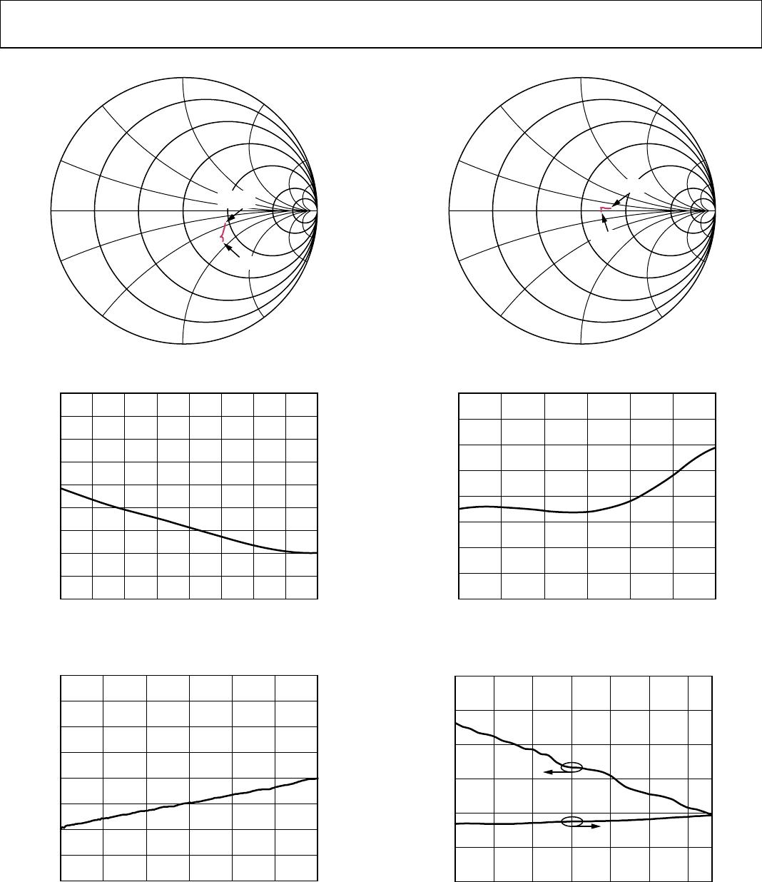
04826-0-040
0180
30
330
10MHz
500MHz
60
90
270
300
120
240
150
210
Figure 37. IF Port Reflection Coefficient from 10 MHz to 500 MHz
IF PORT
The IF port uses an open collector differential output interface.
The NPN open collectors can be modeled as high impedance
current sources. The stray capacitance associated with the IC
package presents a slightly capacitive source impedance as in
Figure 37. In general, the IFOP and IFOM output ports can be
modeled as current sources with an impedance of ~10 kΩ in
parallel with ~1 pF of shunt capacitance. Circuit board traces
connecting the IF outputs to the load should be narrow and
short to prevent excessive capacitive loading. In order to main-
tain the specified conversion gain of the mixer, the IF output
ports should be loaded into 200 Ω. It is not necessary to attempt
to provide a conjugate match to the IF port output source
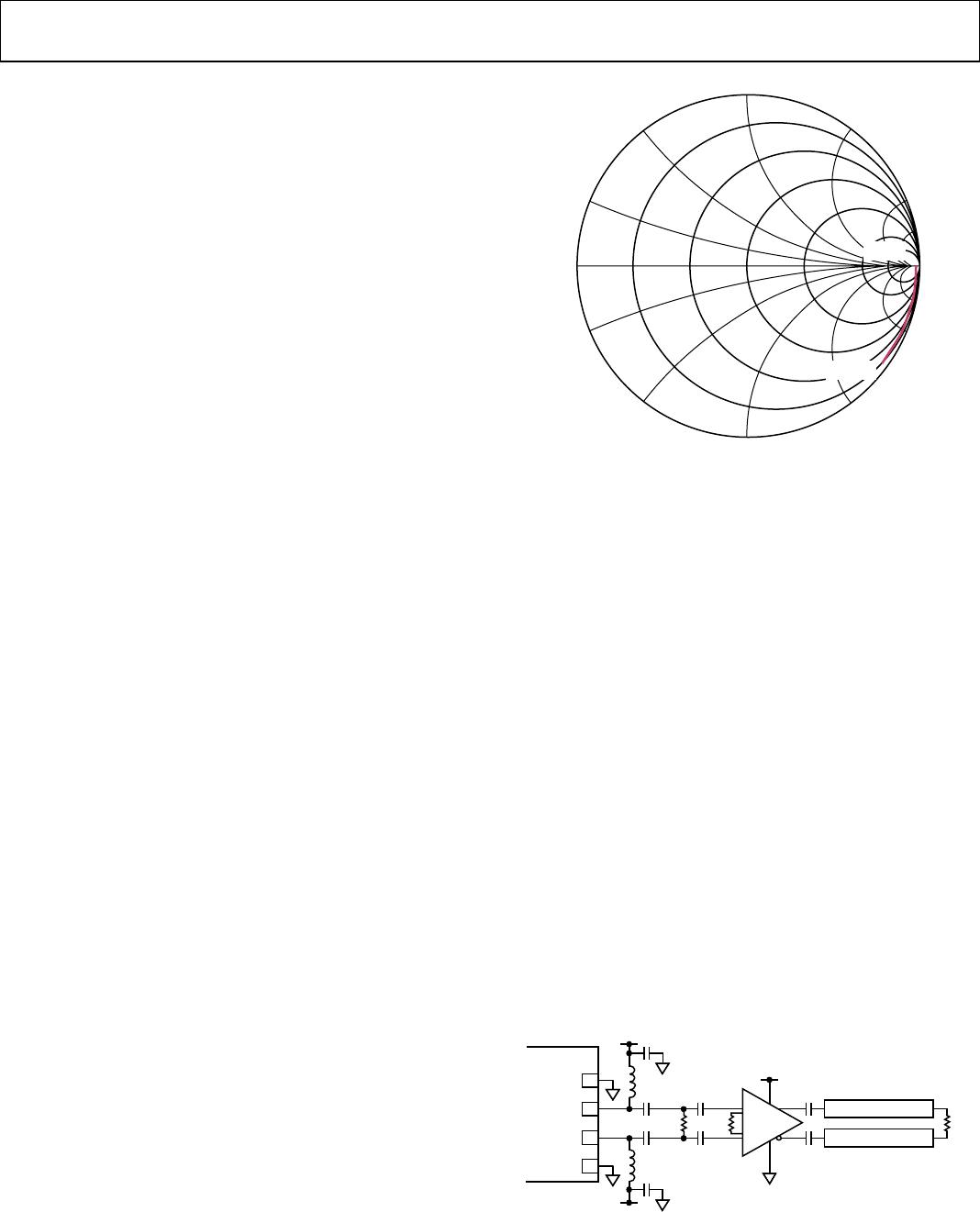
impedance. If the IF signal needs to be delivered to a remote
load, more than a few centimeters away, it may be necessary to
use an appropriate buffer amplifier to present a real 200 Ω load-
ing impedance at the IF output interface. The buffer amplifier
should have the appropriate source impedance to match the
characteristic impedance of the selected transmission line. An
example is provided in Figure 38, where the AD8351 differential
amplifier is used to drive a pair of 75 Ω transmission lines. The
gain of the buffer can be independently set by choosing an
appropriate gain resistor, R
G
.
04826-0-041
COMM
8
IFOP
7
IFOM
6
COMM
5
AD8344
AD8351
+
R
F
C
+
V
S
R
F
C
Z
L
=
2
0
0
+
V
S
+
V
S
200 R
G
Z
L
Tx LINE Z
O
= 75
Tx LINE Z
O
= 75
Figure 38. AD8351 Used as Transmission Line Driver and Impedance Buffer

AD8344ACPZ-REEL7

Mfr. #:
Manufacturer:
Analog Devices Inc.
Description:
RF Mixer IC 400MHz - 1.2GHz Active Receive
Lifecycle:
New from this manufacturer.
Delivery:
DHL FedEx Ups TNT EMS
Payment:
T/T Paypal Visa MoneyGram Western Union

Products related to this Datasheet