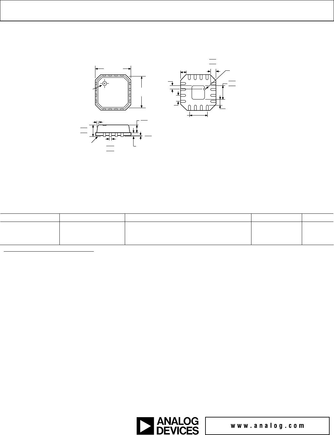
AD8344
Rev. 0 | Page 18 of 20
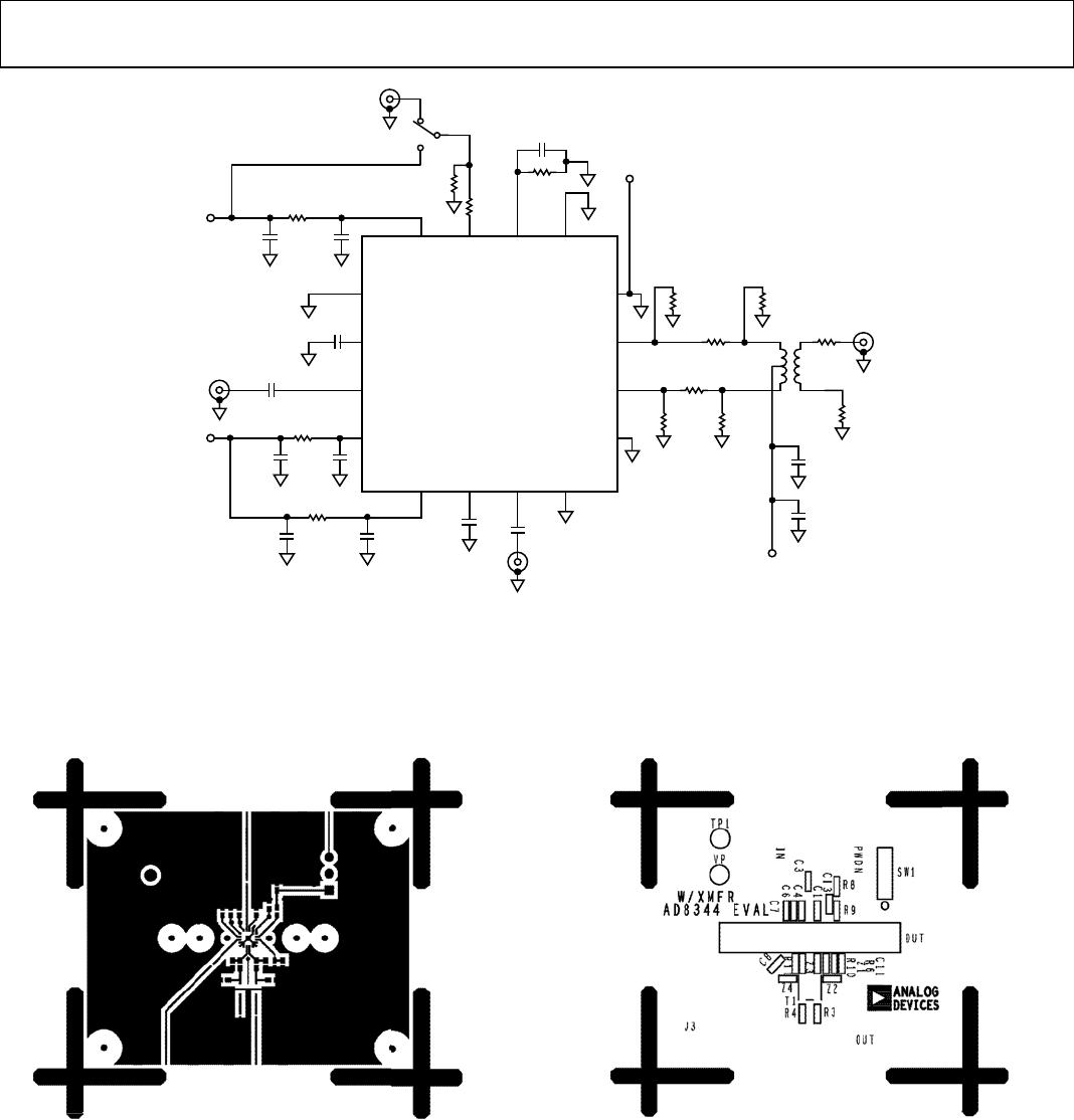
EVALUATION BOARD
An evaluation board is available for the AD8344. The evaluation
board is configured for single-ended signaling at the IF output
port via a balun transformer. The schematic for the evaluation
board is presented in Figure 48.
Table 5. Evaluation Boards Configuration Options
Component Function Default Conditions
R1, R2, R7,
C2, C4, C5, C6,
C12, C13, C14,
C15
Supply Decoupling.
Jumpers or power supply decoupling resistors and filter capacitors.
R1, R2, R7 = 0 Ω (Size 0603)
C4, C6, C13, C14 = 100 pF
(Size 0603)
C2, C5, C12, C15 = 0.1 µF
(Size 0603)
R3, R4 Jumpers in Single-Ended IF Output Circuit. 0 Ω (Size 0603)
R6, C11
R
BIAS
resistor that sets the bias current for the mixer core.
The capacitor provides ac bypass for R6.
R6 = 2.43 kΩ (Size 0603)
C11 = 100 pF (Size 0603)
R8 Jumper for pull down of the PWDN pin. R8 = 10 kΩ (Size 0603)
R9 Jumper. R9 = 0 Ω (Size 0603)
C3
RF Input AC Coupling. Provides dc block for RF input.
C3 = 100 pF (Size 0402)
C1
RF Common AC Coupling. Provides dc block for RF input common connection.
C1 = 100 pF (Size 0402)
C8
LO Input AC Coupling. Provides dc block for the LO input.
C8 = 100 pF (Size 0402)
C7
LO Common AC Coupling. Provides dc block for LO input common connection.
C7 = 100 pF (Size 0402)
SW1
Power Down. The part is on when the PWDN is connected to ground via SW1.
The part is disabled when PWDN is connected to the positive supply (V
S
) via SW1.
T1
IF Output Balun Transformer. Converts differential, high impedance IF output
to single-ended. When loaded with 50 Ω, this balun presents a 200 Ω load to the
mixers collectors. The center tap of the primary is used to supply the bias voltage
(V
S
) to the IF output pins.
T1 = TC4-1W, 4:1 (Mini-Circuits)
R11, Z3, Z4
R12, Z1, Z2
IF Output Interface—IFOP, IFOM. These positions can be used to modify the
impedance presented to the IF outputs.
R11 = 0 Ω (Size 0603)
Z3, Z4 = Open
R12 = 0 Ω (Size 0603)
Z1, Z2 = Open